 Anders Helgesson
I looked at how to erase the NVRAM in the GreenPAK(SLG46826) and I found this.
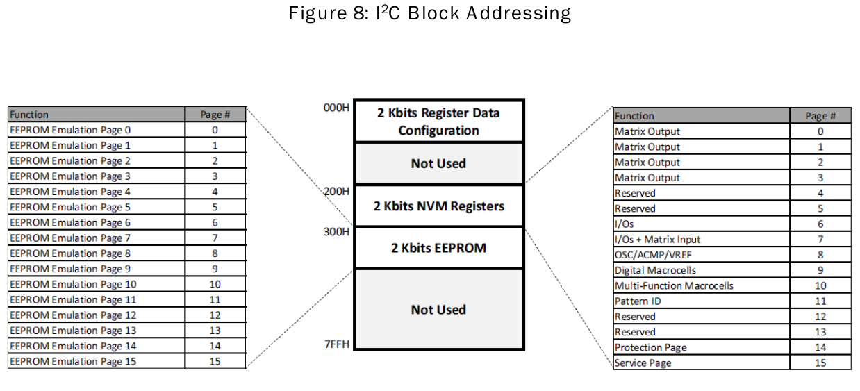
This was not included in the datasheet but in another document (In-System Programming Guide for SLG46824/6/7-A).
This is interesting as my software writes to all but the last service page. I found this table and it tells me that writing to the reserved pages could also be skipped. I'll put it in the comments for the write command for now.
I need to erase pages 0-3 and 6-11. I can skip the reserved, protection and service pages.
Erasing the NVRAM is done through the ERSE register. It is also used to erase the emulated eeprom. The datasheet says "The ERSR register is located on I2C Block Address = 000b, I2C Word Address = E3H."
The ERSE Register (E3H) Bit Function Description looks like this.
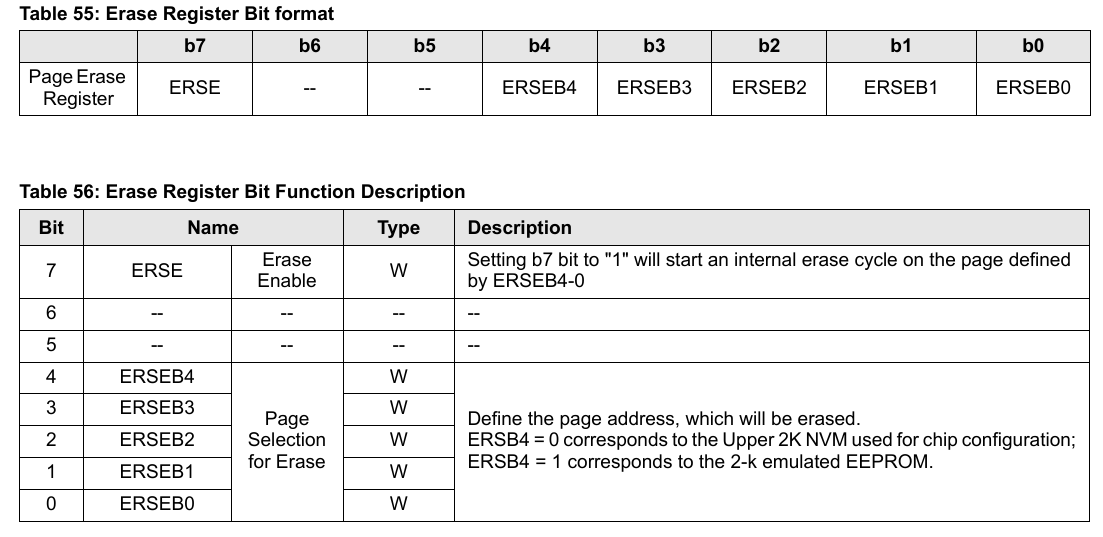
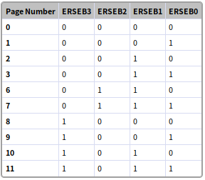
If I understand it correctly the ERSEB3 - ERSEB0 are used like this to set which page that should be erased.
The last 4 bits must be used to select a page number from 0-15. No mention of this but I assume it is how it works.
So for example 10001011b would erase NVRAM page 11, 10011011b would erase emulated EEPROM page 11. I might have mentioned before that the emulated EEPROM can not be used by the GreenPAK it self but could be accessed through I2C to store calibration and other settings that do not change. It also has the limitation of 1000 writes like the NVRAM.
Datasheet notes also says:
"Upon receipt of the proper Device Address and Erase Register Address, the SLG46824/6/7-A will send an ACK. The device will then be ready to receive Erase Register data. The SLG46824/6/7-A will respond with a non-compliant I2C ACK after the Erase Register data word is received. Please reference the SLG46824/6/7-A errata document (revision XC) posted on Renesas’s website for more information.
The addressing device, such as a Bus Master, must then terminate the write operation with a Stopcondition. At that time, the GPAK will enter an internally self-timed erase cycle, which will be completed within tER (max 20 ms). While the data is being written into the Memory Array, all inputs, outputs, internal logic, and I2C access to the Register data will be operational/valid. After the erase has taken place, the contents of ERSE bits will be set to "0" automatically. Erase will be triggered by Stop Bit in I2C command."
I guess I have to take that into account when writing my nvram erase command.
It also says:
"An Acknowledge Polling routine can be implemented to optimize time sensitive applications that would prefer not to wait the fixed
maximum write cycle time (tWR) or erase maximum cycle time (tER). This method allows the application to know immediately when the Serial EEPROM emulation write/erase cycle has completed, so a subsequent operation can be started.
Once the internally self-timed write/erase cycle has started, an Acknowledge Polling routine can be initiated. This involves repeatedly sending a Start condition followed by a valid Device Address byte (NVM block address) with the R/W bit set at Logic 0. The device will not respond with an ACK while the write cycle is ongoing. Once the internal write/erase cycle has completed, emulated EEPROM will respond with an ACK, allowing a new read, erase, or write operation to be immediately initiated.
The length of the self-timed write cycle (tWR) and self-timed erase cycle (tER) is defined as the amount of time from the Stop condition that begins the internal write operation to the Start condition of the first Device Address byte that includes NVM address(A9 = 1; A8 = X) sent to the SLG46826 that it subsequently responds to with an ACK."
I could use this to make the erase command quicker instead of waiting for 21ms per page erase. I guess since some values are already 0 a page erase would take less than the max of 20ms specified in most cases.
Before I had problems with setting the first 2-bit LUT0, maybe the erase command will make it useable? I could read from it but not set it in both NVRAM and in the registers directly. If I need a 3-bit lut I'll try to use the 2-bit LUT0 again for the keypad scanning.
My GreenPAK programming software has no user interface or CLI commands, I lazyly just uncomment commands I want and do cargo run.
It would be way easier if I owned the offical debug probe but it's expensive and got more expensive lately. I built my own barebone one. Only drawback is it doesn't work with the offical software, so I just read the register data directly from the project file instead. It works fine and I can choose to write to either the registers or NVRAM.
With this research complete it's time to implement the NVRAM erase function.
Discussions
Become a Hackaday.io Member
Create an account to leave a comment. Already have an account? Log In.