Additional Notes for Session 1 : KiCad + FreeCAD
GIT REPO
Here's a link to my GIT repo for review.
https://github.com/wyolum/HackadayU_KiCad_FreeCAD
VIEW FOOTPRINT IN SCHEMATIC LIBRARY BROWSER
In EEschema Library Browser, if you see only the schematic symbol but not the footprint, check this setting :
PREFERENCES > PREFERENCES > Eeschema > Show footprint previews in library browser (check)
USE REPETITION FOR SPEED
If you have a bunch of repetitive actions to be done, such as placing incremental net labels, or the same length of wire connected to a succession of pins on an IC, then
- Set up Repetition parameters in
PREFERENCES > PREFERENCES > EEschema
- Set Horizontal pitch of repeated items
- Set Vertical pitch of repeated items
- Place the first item (net label, wire etc).
- Hit the “Insert” key and the item you placed will be repeated according to the parameters set in Preferences. If it’s a Net Label, it will also increment each time you “Insert”.
- Here’s a short video showing how it works.
BUSES
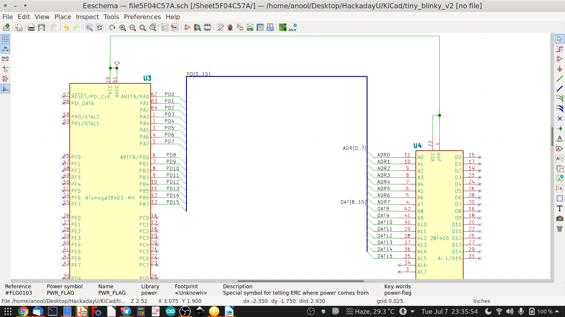
We looked at a super simple example of how busses can be used, it wasn’t exactly an appropriate use of the feature, since the same result can be achieved just by using Net Labels. But for example, if you have a more complex circuit, where there is a 16-bit data bus on a micro-controller labelled PD0..PD15, that needs to be connected to a memory device with 8 pins labelled ADR0..ADR7 and the other 8 pins labelled DAT8..DAT15, then the BUS feature solves the problem.
- Add wire stubs and bus entries on the first device (use the repetition feature to speed things up).
- Add wire stubs and bus entries on the second device
- Add net labels on the first device – PD0 to PD15
- Add net labels to the second device – ADR0 to ADR7 and DAT8 to DAT15
- Draw a bus that connects all of these pins
- Add a net label near the first device – PD[0..15]
- Add a net label near the second device – ADR[0..7]
- Add a third label near the second device – DAT[8..15]
The pins then get connected like so :
PD0 > ADR0
PD1 > ADR1
.....
PD7 > ADR7
PD8 > DAT8
PD9 > DAT9
.....
PD15 > DAT15
Here's a screenshot of how that looks

IGNORE SCHEMATIC SYMBOL
If you'd like to add a symbol on the schematic which should not be placed on the PCB, then add a "hashtag" to it's REFERENCE (example - #U4 instead of U4, and it will not be put on the PCB)
This can be used to show where off-board parts such as a Motor, Fan, Solenoid etc connect to a screw-connector on the board, for example.
KiCad CHEAT SHEET
Handy KiCad cheat sheet for reference, in several languages
https://github.com/KiCad/kicad-doc/tree/master/src/cheatsheet
And here's the link to the KiCad forum if you'd like to give feedback to the author
https://forum.kicad.info/t/cheatsheet-for-kicad/5247
 Anool Mahidharia
Discussions
Become a Hackaday.io Member
Create an account to leave a comment. Already have an account? Log In.
Thanks, @Varun Mehta
Are you sure? yes | no
Thanks for a good first session, Anool! Since you're in IST and I'm in EDT, I think it's great to use pre-recorded sessions for the bulk of course content. I've used KiCad for some tiny projects before, but even in session one I learned a few tips that are helpful. I'm looking forward to the rest of the course!
Are you sure? yes | no