 Dan Maloney
OK, here we go! Welcome to Hack Chat, I'm Dan and I'll be modding along with Dusan today. We're really pleased to welcome John McMaster onto the Hack Chat today to talk about decapping stuff. I'm not sure I've seen John log in yet, though - you out there, John?
 HI all ! No video so ?
 testing.
(sorry for that dumb question, newbie here)
 Hello everyone :-)
 No, no video today. Just good old text
![]() I'm here!
I'm here!
Ok fine, thanks @Dan Maloney !
is there a one to one relationship between MVRVE members and chat participants today?
Hey John, welcome! Thanks for coming on today - can you kick us off with a little on your background?
![]() Sure...Hi all! My name is John McMaster. I'm am embedded systems consultant by day and by night I explore the mysteries of what's inside computer chips.
Sure...Hi all! My name is John McMaster. I'm am embedded systems consultant by day and by night I explore the mysteries of what's inside computer chips.
![]() also, possibility to use lasers for ablation or localized heating of acid drop. (near-IR or visible diode lasers shine through test tubes, too. CO2 is stopped by glass.)
also, possibility to use lasers for ablation or localized heating of acid drop. (near-IR or visible diode lasers shine through test tubes, too. CO2 is stopped by glass.)
![]() I have a garage lab where I decap (open up) computer chips and also have high power microscopes to see the small circuitry
I have a garage lab where I decap (open up) computer chips and also have high power microscopes to see the small circuitry
![]() @Thomas Shaddack are you asking if I do this today or if I've considered it? I did get a laser recently I wanted to use for more precise and quicker silver epoxy curing
@Thomas Shaddack are you asking if I do this today or if I've considered it? I did get a laser recently I wanted to use for more precise and quicker silver epoxy curing
![]() This would in theory let me build up wires a lot more effectively without a bonding machine
This would in theory let me build up wires a lot more effectively without a bonding machine
So actually making "wires" from conductive epoxy?
![]() Yeah. You can get pretty good results but it does require good hand eye coordination if you want to not short out adjacent bond pads. I steady by hand against a shelf which helps al ot
Yeah. You can get pretty good results but it does require good hand eye coordination if you want to not short out adjacent bond pads. I steady by hand against a shelf which helps al ot
![]() a lot
a lot
![]() Also I do this under a microscope
Also I do this under a microscope
Can such wires "fly" like regular bond wires? Or do they need some kind of support?
![]() I've done both. But generally its easier to attach them a short distance to either the existing wire (say if it was old/broken) or add a new one a short distance from the pad
I've done both. But generally its easier to attach them a short distance to either the existing wire (say if it was old/broken) or add a new one a short distance from the pad
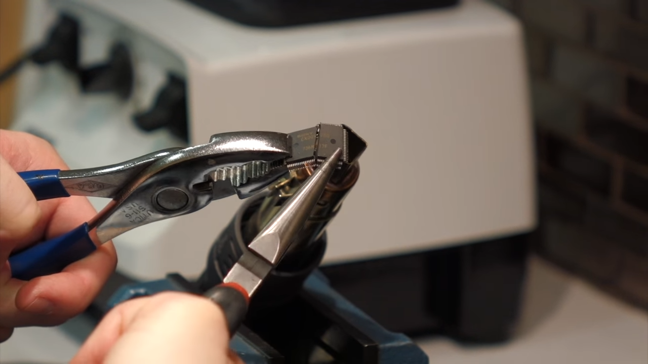
![]() what are you using for decapping?
what are you using for decapping?
So you are decaping ICs yet still trying to keep them alive ?
 ^ yeah! and if so how much runtime can you get?
![]() Depends on the project. If you want to understand just how the chip works its usually not required and often the chip is ultimately destructively analyzed. But if I want some data out I may want to keep it alive so I can do some open heart surgery
Depends on the project. If you want to understand just how the chip works its usually not required and often the chip is ultimately destructively analyzed. But if I want some data out I may want to keep it alive so I can do some open heart surgery
 Does that mean that sometimes you can get the chip running and operating while currently decapped with the silicon visible?
![]() @morgan if done properly it should not significantly harm the chip / normal lifetime
@morgan if done properly it should not significantly harm the chip / normal lifetime
 Hi
Hi
oh neat, was thinking you'd have to gas back or something
![]() @Usagi Electric (David) yup! For some rare chips I've done this and I've heard they still work years later
@Usagi Electric (David) yup! For some rare chips I've done this and I've heard they still work years later
![]() Doesn't dust collecting on the bare die ever cause capacitive problems?
Doesn't dust collecting on the bare die ever cause capacitive problems?
![]() @morgan well some special applications have hermetically sealed packages, but that's more of a harsh environment / reliability thing than the silicon immediately dying. If you are nice to it, it will be fine
@morgan well some special applications have hermetically sealed packages, but that's more of a harsh environment / reliability thing than the silicon immediately dying. If you are nice to it, it will be fine
what about NMOS or PMOS? sure. we pretty much only see CMOS these days, but do you ever scrape the top off old chips? how is decapping an old chip different than decapping a modern chip?
![]() @devinsbench not that I've seen but I'm sure there are exceptions for high speed stuff. Usually large digital ICs at least have top metal with power routing (big metal planes). This essentially provides a shield against most effects
@devinsbench not that I've seen but I'm sure there are exceptions for high speed stuff. Usually large digital ICs at least have top metal with power routing (big metal planes). This essentially provides a shield against most effects
Wild! I never thought that would have been possible. Follow up question(s), is there any detrimental side effect to running with the die exposed (capacitance, influence from mains in the air, heat, etc.), and when running under heavy load under microscope, can you visibly see any changes in the silicon (color, shape?)
![]() hi @brUh__n0mArs !
hi @brUh__n0mArs !
![]() @Meadhbh Hamrick the packaging is very different. For example, modern "flip chips" may have solder balls attached more or less directly to the silicon vs older chips had bond wires going to the package. Let me see if I can find some photos...
@Meadhbh Hamrick the packaging is very different. For example, modern "flip chips" may have solder balls attached more or less directly to the silicon vs older chips had bond wires going to the package. Let me see if I can find some photos...
@Usagi Electric (David) - I had the same question -- do transistors emit some incidental, faint light?
![]()

I mostly just think it would be epic to see the chip pulsing like a beating heart, haha
![]() @Meadhbh Hamrick see the top vs middle? Very different layout. One issue for example is I can image the top one without destroying too much, but the middle one I'd have to be a lot more invasive
@Meadhbh Hamrick see the top vs middle? Very different layout. One issue for example is I can image the top one without destroying too much, but the middle one I'd have to be a lot more invasive
![]() @Usagi Electric (David) thermal issues definitely come to mind. As an extreme case if you back thin the die it can become quite severe. But especially once you start removing heat spreaders or other metal it can be very detrimental to how much power you can put through a die
@Usagi Electric (David) thermal issues definitely come to mind. As an extreme case if you back thin the die it can become quite severe. But especially once you start removing heat spreaders or other metal it can be very detrimental to how much power you can put through a die
sweet
![]() @Dan Maloney yes! I did a talk on this a few years ago, let me find a link
@Dan Maloney yes! I did a talk on this a few years ago, let me find a link
![]()
https://www.hardwear.io/usa-2019/speakers/john-mcmaster.php

Infrared Light for Reverse Engineering | hardwear.io USA 2019
Talk Title: Infrared Light for Reverse Engineering Abstract: Traditionally integrated circuits are reversed engineered by imaging transistors and analyzing their structure to determine logic function. Instead, this talk explores correlating infrared emissions to logic functions. While traditionally prohibitively expensive, relatively low cost techniques are presented to make this more approachable to a typical lab.
 This is the recording of that talk, I believe:
![]() slides: https://docs.google.com/presentation/d/1J8pTBp_aQNc8Kdejf8dk0_q8NulvI5OzNmjMV_7zyug/edit#slide=id.p
slides: https://docs.google.com/presentation/d/1J8pTBp_aQNc8Kdejf8dk0_q8NulvI5OzNmjMV_7zyug/edit#slide=id.p
![]() thanks @James Gerity !
thanks @James Gerity !
Man, that's wild. Guess it makes sense, though -- different parts of the chip will heat more when they're used more.
![]() But yeah I have a special microscope for that. I did something really fun with that setup recently, hopefully I'll give a talk on it in the near future but I'm being a bit hush about it now
But yeah I have a special microscope for that. I did something really fun with that setup recently, hopefully I'll give a talk on it in the near future but I'm being a bit hush about it now
![]() @Dan Maloney my understanding of physics is a bit limited but I believe in this case though its not heating energy so much as holes recombining
@Dan Maloney my understanding of physics is a bit limited but I believe in this case though its not heating energy so much as holes recombining
Even wilder...
![]() :)
:)
Just flipped through the slides, that's insane work, really excellent stuff. I'll have to watch the vid on the talk later!
![]() thanks!
thanks!
Charge carrier-hole recombination is the mechanism I'd expect there. Never expected to see it in this context, though. Extremely cool stuff
![]() An interesting tidbit regarding heat spreading I've learned is that if you take any old wire and and put enough current through it for it to break, You'll always find the break right in the middle of the wire because of heat sinking. You could apply that to the interconnection layer of an IC, probably.
An interesting tidbit regarding heat spreading I've learned is that if you take any old wire and and put enough current through it for it to break, You'll always find the break right in the middle of the wire because of heat sinking. You could apply that to the interconnection layer of an IC, probably.
So, what is the weirdest/strangest chip you've ever decapped?
Hi John, sorry, I'm in share phone connection.. is not so good, but I'm reading the messages..
![]() @Usagi Electric (David) Hmm...well I decapped a radiation hardened FPGA once. Shortly after I learned that I probably ground up some beryllium alloy to get it open. Oops
@Usagi Electric (David) Hmm...well I decapped a radiation hardened FPGA once. Shortly after I learned that I probably ground up some beryllium alloy to get it open. Oops
Nasty stuff. Any ill effects?
![]() Nope
Nope
![]() I was supposed to decap a Commodore 65 CPU but e-mails went back and forth for a long time and the chip ultimately didn't show up, but that would have been quite rare
I was supposed to decap a Commodore 65 CPU but e-mails went back and forth for a long time and the chip ultimately didn't show up, but that would have been quite rare
![]() I've done some security modules that are pretty involved. Now I'm doing some consulting helping people design HSMs so its fun to be on the other side
I've done some security modules that are pretty involved. Now I'm doing some consulting helping people design HSMs so its fun to be on the other side
Dang, what entails radiation hardening?
I think you should open a hands on course, basic. To teach a setup lab, basic and cheap tools, and then an advanced course to teach the tricks.
![]() @Usagi Electric (David) hmm for legal reasons (ITAR) I'd rather not get too much into that
@Usagi Electric (David) hmm for legal reasons (ITAR) I'd rather not get too much into that
For a cheap price, to have more people involved.
Haha, no worries!
@Usagi Electric (David) a lot of concern for aerospace is resiliency to single-event events (SEE). Can you survive a single energetic proton or cosmic ray and recover, basically.
err, single-event effects*
![]() For background though I did a large portion of my career in aerospace. I still do radiation testing consulting sometimes for satellites
For background though I did a large portion of my career in aerospace. I still do radiation testing consulting sometimes for satellites
![]() @JohnDMcMaster maybe you should get in touch with Scotty from Strange Parts. He got a new scanning electron microscope and wanted to check some ICs, but was a bit reluctant to mess with the decaping process
@JohnDMcMaster maybe you should get in touch with Scotty from Strange Parts. He got a new scanning electron microscope and wanted to check some ICs, but was a bit reluctant to mess with the decaping process
![]() Where I used a cyclotron to make a furby so radioactive it had to go into decontamination to cool down for a month. I got a really dirty look from their RSO (radiation safety officer)
Where I used a cyclotron to make a furby so radioactive it had to go into decontamination to cool down for a month. I got a really dirty look from their RSO (radiation safety officer)
wait. rad hardening is covered by ITAR? uh oh.
Haha, I was wondering about that furby when I saw another video, immediately thought of friends who work on a cyclotron with a private-use SEE line
That is one hot Furby!
@Meadhbh Hamrick a lot of the use-cases are well into that territory, yep
![]() @hexpwn oh nice! Yeah I know Scotty. I actually knew him from a while back and didn't connect it was the same guy until we met up at Defcon a few years ago
@hexpwn oh nice! Yeah I know Scotty. I actually knew him from a while back and didn't connect it was the same guy until we met up at Defcon a few years ago
Reminds me of a tip we got yesterday:
https://en.wikipedia.org/wiki/Anatoli_Bugorski

Anatoli Bugorski
Anatoli Petrovich Bugorski (Russian: Анатолий Петрович Бугорский), born 25 June 1942, is a retired Russian particle physicist. He is known for surviving an accident in 1978, when a high energy proton beam from a particle accelerator passed through his brain.
![]() He also offered to help me with Youtube, but I'm not as serious as him and am just messing around
He also offered to help me with Youtube, but I'm not as serious as him and am just messing around
Might be a bit unrelated, but do you find that military/aerospace grade electronics differ heavily from consumer grade electronics from a silicon standpoint?
![]() @Usagi Electric (David) I'll let others handle that
@Usagi Electric (David) I'll let others handle that
![]() @Dan Maloney classic! Yeah I'll try not to be that guy
@Dan Maloney classic! Yeah I'll try not to be that guy
![]() @JohnDMcMaster That's cool that you know each other! Maybe a youtube colab would be cool :D I suggested he poke the new RP2040 chip from Raspberry foundation (used in their new Pico board). It has some cool Programable IO features and I'm very curious how it looks under the resin :)
@JohnDMcMaster That's cool that you know each other! Maybe a youtube colab would be cool :D I suggested he poke the new RP2040 chip from Raspberry foundation (used in their new Pico board). It has some cool Programable IO features and I'm very curious how it looks under the resin :)
Hah, I keep asking questions that need a security clearance
![]() @hexpwn I presume you saw the quick teardown I did? https://twitter.com/johndmcmaster/status/1355092011829719046
@hexpwn I presume you saw the quick teardown I did? https://twitter.com/johndmcmaster/status/1355092011829719046
![]() I have a stack of bare RP2040 chips here now though if someone has ideas for them
I have a stack of bare RP2040 chips here now though if someone has ideas for them
The banner image on the event page was an RP2040, I believe: https://hackaday.io/event/177772-decapping-components-hack-chat-with-john-mcmaster
![]() @Dan Maloney yes it is!
@Dan Maloney yes it is!
![]() May it rest in peace
May it rest in peace
![]() I missed that 😳
I missed that 😳
I had to crop it, sorry
![]()
https://siliconpr0n.org/map/raspberry-pi/rp2-b0/s1-9_mit20x/
Loading...
![]() Zoomable map
Zoomable map
![]() @hexpwn anyway if someone requested scotty and I to do a video together and it got a lot of likes on twitter or something I'd consider it
@hexpwn anyway if someone requested scotty and I to do a video together and it got a lot of likes on twitter or something I'd consider it
![]() oh that's awesome
oh that's awesome
![]() Otherwise I think too much going on here right now unfortunately
Otherwise I think too much going on here right now unfortunately
You could sell a lab setup basic tools and make a course for who bought the kids, maybe free or you can charge a little donation, and then for who made the 1srcourse you could open advanced* course for a little price or donation. But just who bought the kits and make the baic first setup lab course
![]() I'll keep pestering him to do a video on it with his flashy new SEM :D
I'll keep pestering him to do a video on it with his flashy new SEM :D
![]() :)
:)
"Hey kids ! Let's play with nitric acid !"
![]() Lol yes that is one issue. But there are some safe labs I could help lead like decapping a ceramic chip
Lol yes that is one issue. But there are some safe labs I could help lead like decapping a ceramic chip
Not kids kits :)
Fuming nitric acid? Even more fun
![]() And pair it with one of those $20 USB microscopes
And pair it with one of those $20 USB microscopes
Up to 21 years old
![]() BTW any general requests for chips to be decapped? I keep thinking of doing a series on LEDs but haven't gotten around to it
BTW any general requests for chips to be decapped? I keep thinking of doing a series on LEDs but haven't gotten around to it
The "heat and twist" method CuriousMarc showed on his channel seems pretty innocuous too
![]() Do you want more chips?
Do you want more chips?
![]() @devinsbench I'm a hopeless hoarder yes please
@devinsbench I'm a hopeless hoarder yes please
https://hackaday.com/2020/03/11/chip-decapping-the-easy-way/
Chip Decapping The Easy Way
Chip decapping videos are a staple of the hacking world, and few things compare to the beauty of a silicon die stripped of its protective epoxy and photographed through a good microscope. But the process of actually opening that black resin treasure chest seems elusive, requiring as it does a witch's brew of solvents and acids.
![]() @Dan Maloney yeah that can work pretty well if you want something low tech. It does put off fumes though so you need to be a bit careful still
@Dan Maloney yeah that can work pretty well if you want something low tech. It does put off fumes though so you need to be a bit careful still
@Dan Maloney I actually tried that with some spare 74HC chips I had. I stopped after I set my hair on fire
![]() It also has higher risk of breaking chips so I tend to shy away from it
It also has higher risk of breaking chips so I tend to shy away from it
![]() !
!
Actually, that's a question I had -- what's the substance used for chip packages. Is it a plastic or an epoxy?
@Usagi Electric (David) - Does that explain the recent haircut?
Haha, not quite, interestingly, it actually made the long hair more livable as it made my bangs a bit shorter. Though, I would recommend to anyone trying to hot air decap method, do it with hot air and not an open flame like I did!
![]() @Dan Maloney glass filled epoxy resins. I think I have a page on this, sec
@Dan Maloney glass filled epoxy resins. I think I have a page on this, sec
![]() BTW if anyone wants to contribute to http://siliconpr0n.org/ let me know and I'll create you an account
BTW if anyone wants to contribute to http://siliconpr0n.org/ let me know and I'll create you an account
![]() ex if you are interested on improving the page on chip materials
ex if you are interested on improving the page on chip materials
![]()
https://siliconpr0n.org/wiki/doku.php?id=carrier:epoxy
carrier:epoxy [Silicon Pr0n]
There are two common types of epoxy packages: thermoset epoxy used for PDIPs and the like, and epoxy resins used for PGAs. The former are typically dark brown or black and mixed with glass beads, while the latter are typically green, yellow, or brown with layered fiberglass.
Cool, thanks!
John, is there a size limit for the chips you can decap, both too large or too small?
![]() @Usagi Electric (David) strictly for decapping no, but imaging and delayering is a lot more problematic. I'm theoretically limited to about 30 nm right now but in practice you'd want to stay above that (say 60 nm). There is a chance I may get a much better SEM in the near future though
@Usagi Electric (David) strictly for decapping no, but imaging and delayering is a lot more problematic. I'm theoretically limited to about 30 nm right now but in practice you'd want to stay above that (say 60 nm). There is a chance I may get a much better SEM in the near future though
![]() I don't have a good process for delayering modern chips in part because I haven't traditionally worked on them. But I'm starting to do more consulting work on modern chips so that may change over the next year
I don't have a good process for delayering modern chips in part because I haven't traditionally worked on them. But I'm starting to do more consulting work on modern chips so that may change over the next year
Interesting, 60nm is still properly small!
Is lapping of any use in getting into a chip? I seem to recall ElectronUpdate was trying to build a lapping machine from old HDDs at one time.
Why we don't see deap of processors like xeon or ryzen?
Decap
![]() @Dan Maloney I have pretty nice lapping equipment here, but some combination of needing to practice and not doing enough modern chips I haven't been using it heavility
@Dan Maloney I have pretty nice lapping equipment here, but some combination of needing to practice and not doing enough modern chips I haven't been using it heavility
 I'd think there isn't anything of particular interest in modern 8nm processors...
![]() I might try to extract the RP2040 bootloader with it since I have a stack of them here...we'll see
I might try to extract the RP2040 bootloader with it since I have a stack of them here...we'll see
![]() @brUh__n0mArs there's a lot of demand to deacp things but my time is relatively limited. I focus on chips that have some sort of higher impact. Major factors are 1) funding (will someone help cover costs) 2) application (what will get done with the data)
@brUh__n0mArs there's a lot of demand to deacp things but my time is relatively limited. I focus on chips that have some sort of higher impact. Major factors are 1) funding (will someone help cover costs) 2) application (what will get done with the data)
![]() Most of the modern chips are fun to photograph but don't generate a lot of value. So I tend to leave those to people like Antoine and Birdman that are more into that type of photography
Most of the modern chips are fun to photograph but don't generate a lot of value. So I tend to leave those to people like Antoine and Birdman that are more into that type of photography
 For a beginner that doesn't have easy access to nitric acid or fuming nitric acid, is there another way that is non destructive? I have an oddball Intel microprocessor that I would like to reverse engineer, but dont want to destroy the package if possible.
I would like to see a xeon decaped
![]() @Miles Paulson I recommend ceramic packages and shear them open. Either with metal lid or glass frit, both are fairly easy to open
@Miles Paulson I recommend ceramic packages and shear them open. Either with metal lid or glass frit, both are fairly easy to open
![]() @brUh__n0mArs all of them? :)
@brUh__n0mArs all of them? :)
Unfortunately the device I am curious about is only in a plastic package
![]() @Miles Paulson which device?
@Miles Paulson which device?
@Miles Paulson or any TO3 package IC ;)
Intel 8061 or 8065. Only used in ford fuel injection computers from the 80's up to the early 2000s
![]() i'm thinking about experimenting more with mechanical decapping. i can thin the top of a plastic DIP so that there is an extremely thin layer of encapsulant on top of the die, but i can't figure out a good way to remove just that last thin layer
i'm thinking about experimenting more with mechanical decapping. i can thin the top of a plastic DIP so that there is an extremely thin layer of encapsulant on top of the die, but i can't figure out a good way to remove just that last thin layer
![]() it is thin enough that you can see the die through it. maybe heat? some household solvent?
it is thin enough that you can see the die through it. maybe heat? some household solvent?
Oh wow, looked up at the clock and was surprised that it's already 1:00! We like to let our hosts get back to real life after an hour, so let's say thanks to John for his time today. And thanks to everyone for the excellent questions -- great discussion, I learned a lot.
Can be only one.. =]
![]() Thanks for hosting!
Thanks for hosting!
![]() thanks
thanks
Feel free to keep the conversation going, though - hack Chat is always open.
Hi @tubetime - we'll see you next week too:
![]() @Miles Paulson well especially if you are willing to cover decap costs I'm happy to do it for you, time permitting (https://siliconpr0n.org/archive/doku.php?id=mcmaster:start#commissioning)
@Miles Paulson well especially if you are willing to cover decap costs I'm happy to do it for you, time permitting (https://siliconpr0n.org/archive/doku.php?id=mcmaster:start#commissioning)
Discussions
Become a Hackaday.io Member
Create an account to leave a comment. Already have an account? Log In.