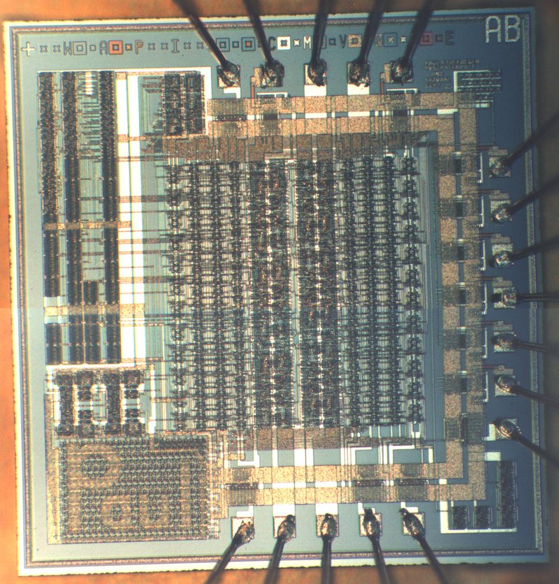
 Thomas Parry did a livestream with me about his process
https://www.zerotoasiccourse.com/post/livestream-with-thomas-parry/
 his day job is analog asic design, so he's good to see how a pro uses the open source tools
 Matt, Thank you for sharing. As you know, chip design is not easy---or everyone would be doing it! :-)
 Any idea how many more shuttles are planned for the free open source stuff? I recall hearing 6 last year. Does #5 going in soon mean there will be only 1 more left?
 Hi Bruce, yes, it's not easy. Personally the long wait is a kller
 i remember improving so rapidly when the open source fpga tools came along and I could iterate on hardware a lot faster
 but mpw1 took a year so now I can learn from the mistakes I made then!
 Hi Paul! at least another 4 this year
 oh, that's good to hear. I still sometimes fantasize about having time for this....
 yeah!
yeah!
 it does take quite a bit of time
![]() does each die contain projects from multiple people + picorv32a?
does each die contain projects from multiple people + picorv32a?
 Yup! I designed a chip 1993, which was made via Mosis. Spent all day and night on it for 3 months!
 wowza
wowza
 Nick, my applications generally combine lots of designs from different people,


 Curious about logistics. Do they just deliver a naked die? If so, how do you put it to work? Or do they do wire bonding and a lead frame, etc?
 but if you take a look at the submitted projects https://platform.efabless.com/projects/public you can see that most are just from a single person or group
 nice one Paul! I still haven't got my name on a die yet!
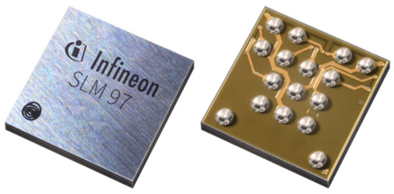
 Dan, no they ship WLCSP at 0.5mm pitch
 we got bare dies on mpw1 because they thought maybe it would help with the bringup
if you don't know, we thought mpw1 was going to be a total write-off
 How did it get "fixed", can you describe what happened?

https://www.zerotoasiccourse.com/post/mpw1-bringup/
MPW1 Bringup
I submitted my first ASIC designs to the free Google shuttle in December of 2020. In October 2021, we heard there were serious clock related problems with the management area of the chip due to issues with the toolchain. It seemed unlikely that anyone would be able to get anything beyond a single blinking LED from MPW1.
Read this on Zero to ASIC Course
 Was it only one fab run?
 I do wish they'd do more maker friendly packages. Like QFN at least
 yeah, not sure why they don't. I heard a few answers, one was price and the other was performance
 but tbh I didn't have too much problem with hot air
 and I think probably that's not a big barrier if you've got to the point of receiving your own chips. Also in the future they'll be delivering a few assembled pcbs along with the rest of the ics
 Tim, no we have had 4 now. 5th is on Monday
 another 4 this year
![]() what package is used?
what package is used?
 WLCSP
WLCSP

https://www.zerotoasiccourse.com/terminology/wlcsp/
WLCSP
Wafer Level Chip Scale Packaging
Read this on Zero to ASIC Course
![]() pin pitch?
pin pitch?
 0.5 mm :)
![]() ouch
ouch
 yeah, it was my finest up to that point
![]() 0.8mm = everyday PCB fab, 0.5mm is more specialized
0.8mm = everyday PCB fab, 0.5mm is more specialized
 we weren't expecting great yield due to the hold timing issues, but I got similar results to Sylvain tnt munaut
so I think my soldering was ok
 just lots of flux and heat
 fwiw, in my dream world of infinite hours in every day for open source, I really wanna try some analog stuff like 12/480 USB PHY and a 10/100 ethernet PHY....
 Nick, I got pcbs from oshpark using their standard service and they looked good
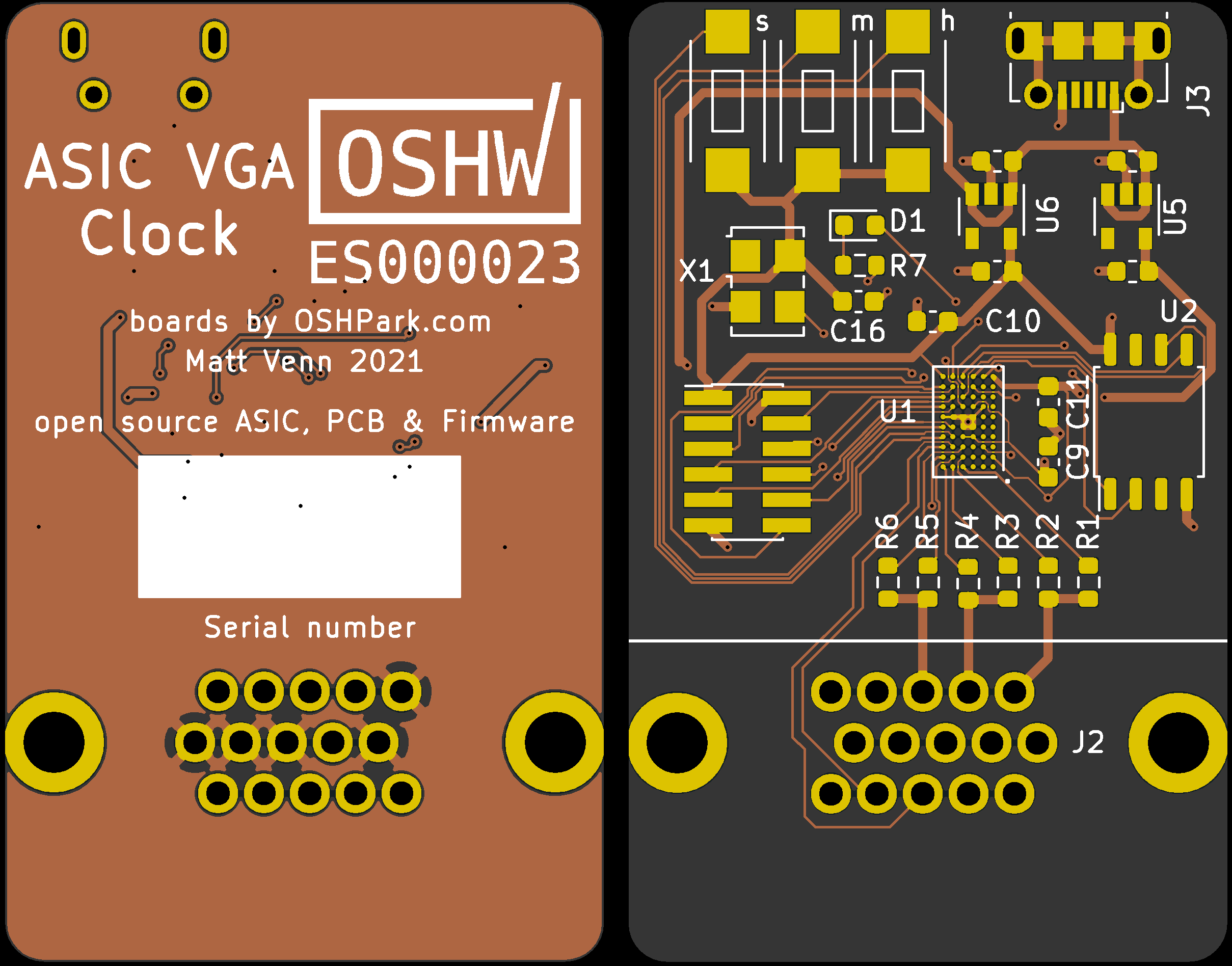
![]() what via hole size + ring size? or were you able to do it without vias under the chip
what via hole size + ring size? or were you able to do it without vias under the chip

https://www.zerotoasiccourse.com/post/vga_clock_pcb/
World's first certified open source hardware down to the chip level?
I'm very pleased to get OSHWA certification for my ASIC clock. Who knows, maybe this is a world first! The clock was submitted as part of MPW1. We're expecting silicon back in August/September, so it was time to get the PCB ready and try to source the other components!
Read this on Zero to ASIC Course
 the 4 centre balls are all ground, so you can put a via there
 so single via
 but yeah, this would be expensive with pcbway
 oshpark let you break the rules, but I checked continuity of all the pads and looked good
![]() are fuse bits possible on this process?
are fuse bits possible on this process?
 We're up past the top of the hour now, so we'll have to let Matt get on with his evening. I just want to say thanks for a great chat -- I sort of followed it, seems like something you just have to dive into to really understand. Matt's course sounds like a great way to get going too. Thanks for the time, Matt! And thanks to everyone for the lively discussion and great questions.
 Nick - I don't know about that
![]() @Nick Kelsey In the Sky130B PDK there is ReRAM. That can be used to make NV memory
@Nick Kelsey In the Sky130B PDK there is ReRAM. That can be used to make NV memory
 Dan, thanks for the invite, and thanks everyone for the questions! Hope to see some of you tape out your first chips in 2022.
 Thanks a lot Matt, it was very helpful and I'll try to get into the course, seems an amazing thing to learn.
 Sounds awesome, appreciate and hope to do a project with your course!
![]() thanks for chatting - I will sign up
thanks for chatting - I will sign up
 join the mailing list for discount codes etc
 Matt, Thanks again for sharing!
 like and subscribe lolz
 Thanks @matt venn for the great chat
 Transcript coming up. Thanks everyone! Taking next week off, but we'll be back on the 30th to talk about thermal design issues for PCBs
 have a great week everyone!
![]() Thanks, Matt!
Thanks, Matt!
 Dan Maloney

Discussions
Become a Hackaday.io Member
Create an account to leave a comment. Already have an account? Log In.