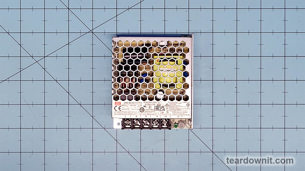

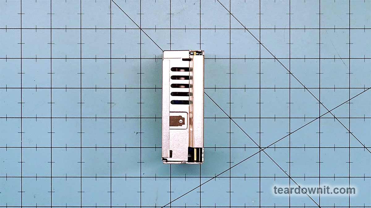
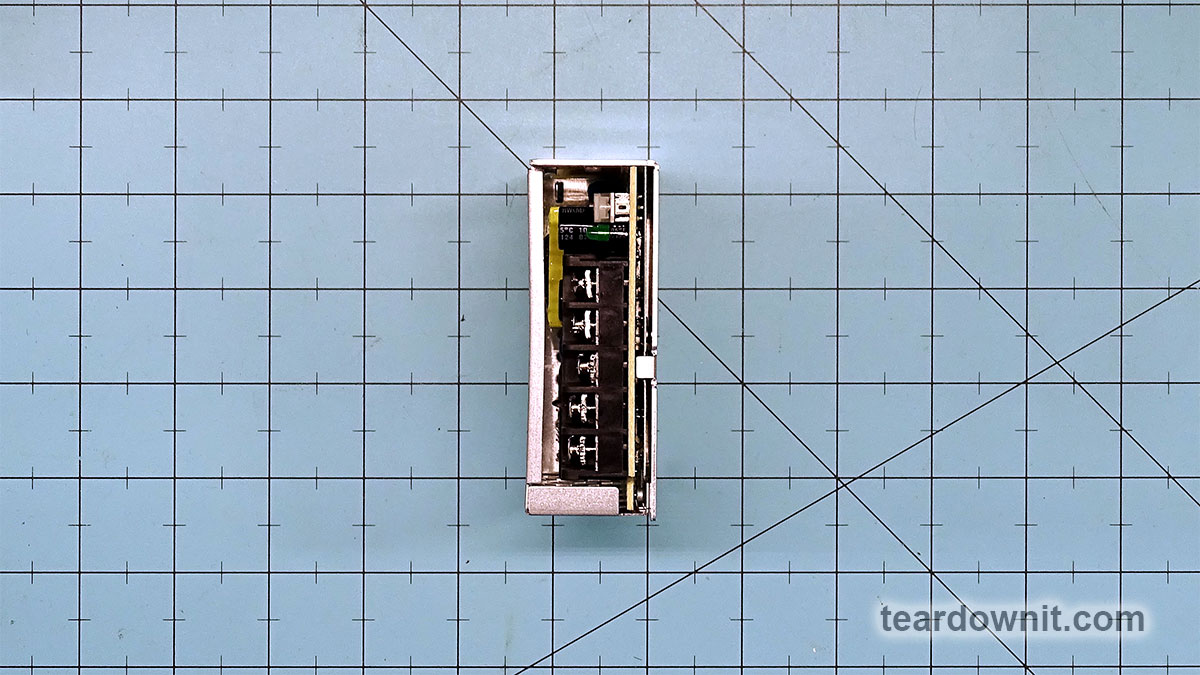
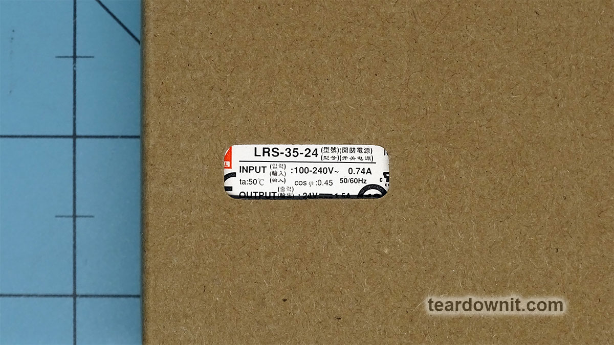
The packaging box is made of cardboard. A small window allows the user to identify the power supply model without removing it from the packaging.

The power supply is built on the TEA18363 chip.
It is a single-cycle DC-DC converter controller from NXP Semiconductors. The chip needs an external n-channel power transistor. The controller is designed for a flyback converter topology and focuses on maximum power efficiency with minimum components. This feature is listed in the datasheet footer: "TEA18363T GreenChip SMPS control IC".
Structural diagram is traditional: input → filter → rectifier bridge → inverse pass converter with rectifier working for output C-L-C filter, regulation by the output voltage, the control signal is transmitted through the optocoupler.
The power supply has no PFC.
Careful assembly of the components. The quality of the connections is good.
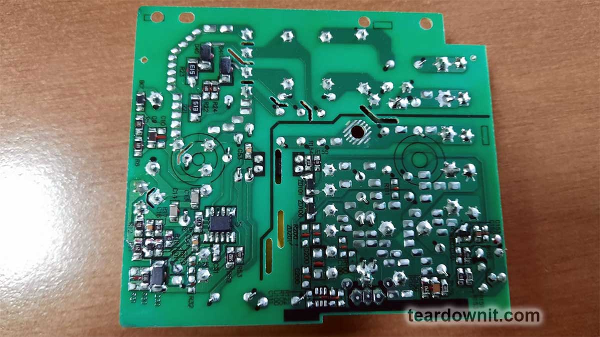
We consider placing the optocoupler, which is practically under the transformer, as a design disadvantage. If this component fails, it won't be easy to replace it.
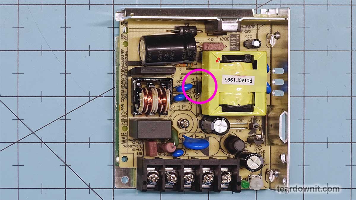
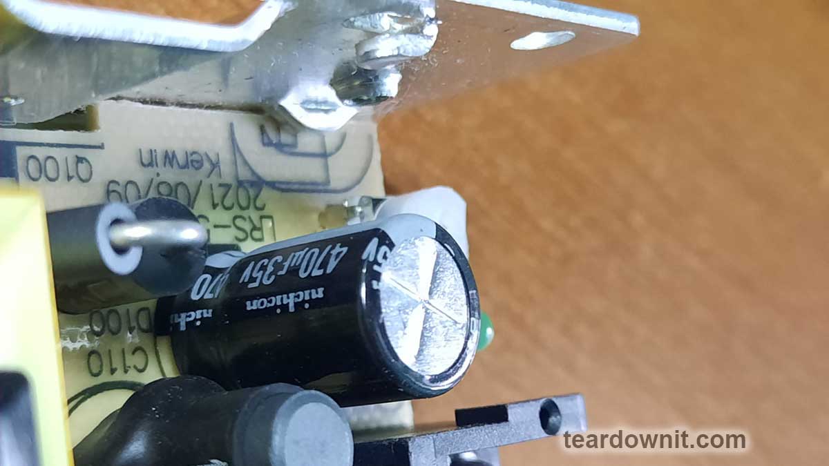
The manufacturer used the output rectifier diode in the DO-201 package (shown with a red arrow in the photo) for an unclear reason. After all, the design provides for a diode with heat dissipation to the metal wall of the unit.
Test results

• The pulsation value as a fraction means that the voltage has pronounced HF (numerator) and LF (denominator) components.
• The hottest component in the power supply is the output rectifier diode. Its temperature is shown in the corresponding table cell.
• The overcurrent protection trips at an output current of 2A and operates in start-stop mode.
What is the "start-stop" mode of protection?
When an overload is detected, the power supply turns off, pauses briefly (usually after 0.5-2 seconds), then tries to turn on again; if it still sees an overload, it turns off again and then goes through the cycle until it finds that the load is back to normal at the next start attempt, after which it resumes regular operation. In the event of damage to the load, this mode reduces the risk of fire and energy loss many times over. This is the reason why this mode is actively used in modern power systems. However, it also makes it impossible for several separate power supplies to operate in parallel for a total load greater than the rated load of one of them.
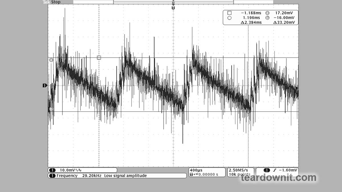
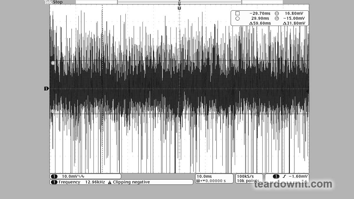
Output voltage pulsations
Slow sweep waveforms
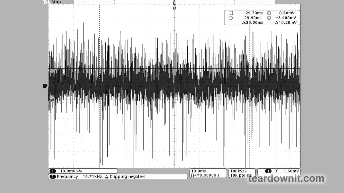
Fast sweep waveforms
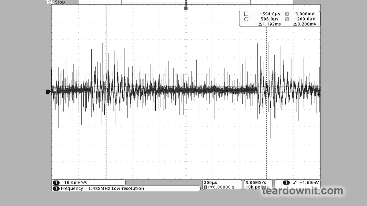
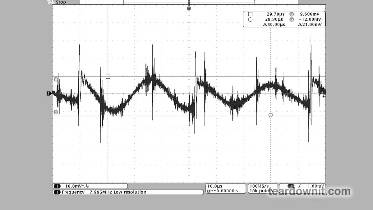
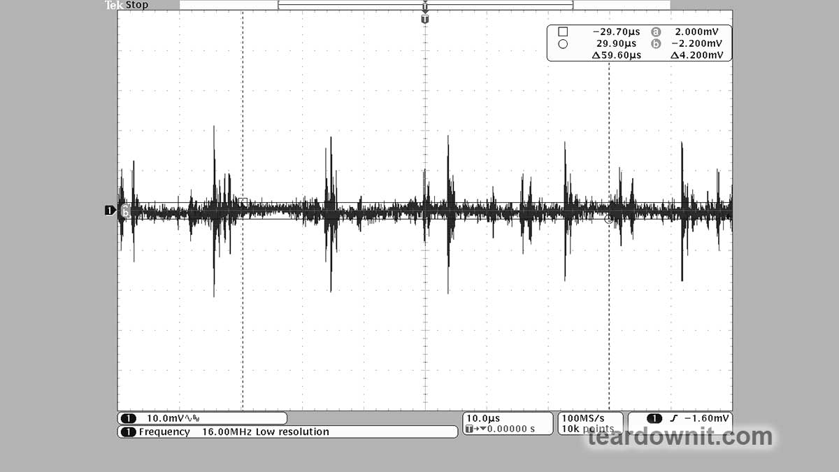
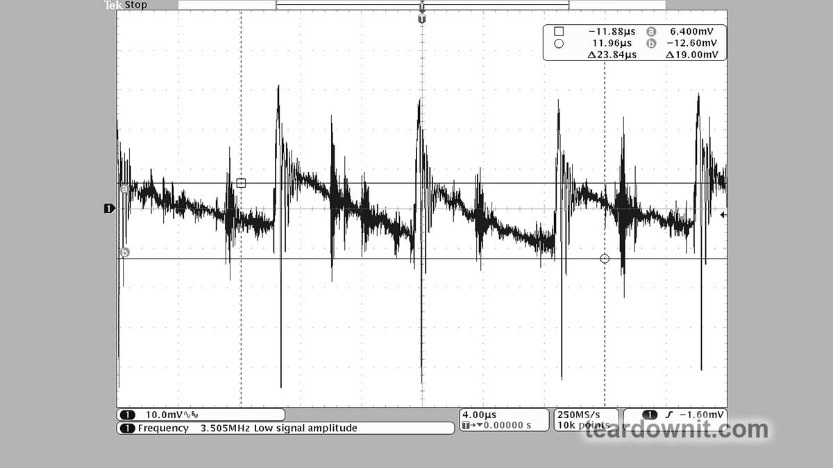
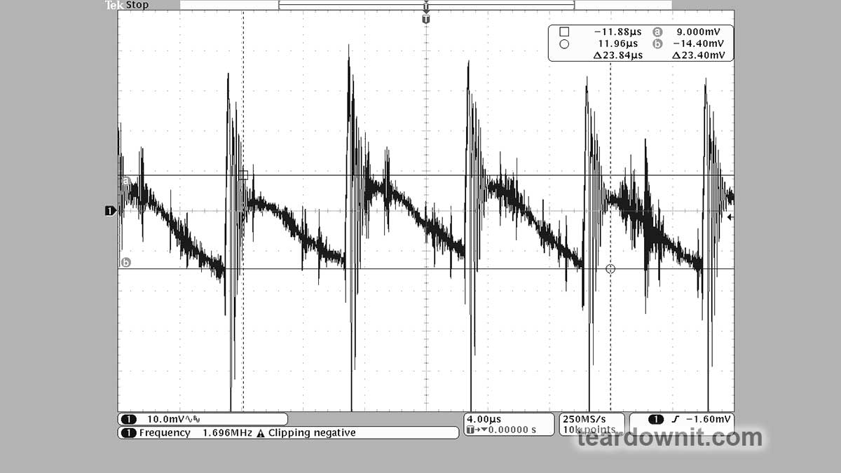
The waveforms clearly show that the converter goes into burst mode in no-load mode. The overall ripple level increases due to an emerging low-frequency component with a peak-to-peak of about 40 mVp-p.
Conclusions
• The output diode is in a heavy thermal mode when the housing is closed. The transition-to-environment thermal resistance of the DO-201 package is high, about 86 °F/W, and at an average output current of 1.5 A, this becomes a problem. Clearly, abandoning the stock diode with heat dissipation to the block wall was a bad idea.
• The power supply can operate at full load for short periods of a few minutes, but the following limits should be observed for the safe and continuous operation of this power supply:
- It is dangerous to operate the unit at a constant full load. At an ambient temperature of 77°F, the output rectifier diode temperature reaches dangerous levels.
- A load reduction of up to 70% allows regular unit operation at ambient temperatures up to 86°F.
• Power supplies of this type cannot be paralleled to work with a load greater than the rated load of one power supply.
 teardownit
Discussions
Become a Hackaday.io Member
Create an account to leave a comment. Already have an account? Log In.