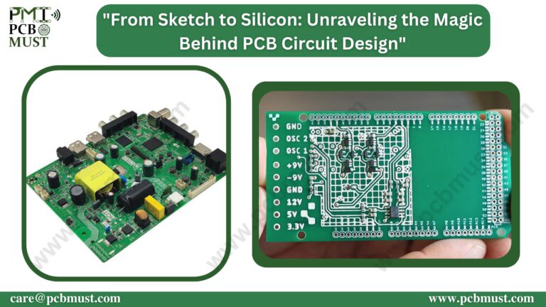
The need for effective and cutting-edge electronic equipment is always rising in today’s fast-paced technological environment. These gadgets, which range from self-driving cars to smartphones, depend on complex electronic circuitry to work properly. The Printed Circuit Board (PCB), a key component in charge of connecting and powering various electrical components, is at the centre of these circuits. To create dependable and high-performing electronic devices, it is essential to comprehend the PCB circuit design process from the original drawing to the finished output. In this thorough book, we will delve into the complex realm of PCB circuit design and examine the essential procedures and ideas needed to turn a simple sketch into a useful and effective PCB.

1. Understanding the Fundamentals of PCB Circuit Design
1.1 PCBs’ Function in Electronics
By providing mechanical support, electrical connections, and signal channels, PCBs act as the brain of electronic gadgets. They make it possible to easily combine different electronic parts, like resistors, capacitors, and integrated circuits, into a dependable and small container. Engineers can assure effective signal flow, reduce electrical noise, and improve the overall performance and dependability of the electronic device by developing an optimised PCB layout.
1.2 Considerations for PCB Design
In order to attain optimal performance, effective PCB design necessitates a methodical approach. Among the most important factors are:
1.2.1 Component Routing and Placement
To preserve signal integrity and reduce interference, proper component location and routing are essential. Signal delays, crosstalk, and electromagnetic interference (EMI) can be reduced by carefully placing components and organising the routing channels.
1.2.2 Power and Ground Planes
Dedicated power and ground plane implementation aids in achieving a steady power distribution and reducing noise. By offering a low impedance channel for current flow and lowering voltage drops, these planes serve as an EMI shield.
1.2.3 Thermal Management
In order to keep electronic components from overheating, effective thermal management is essential. The lifetime and dependability of the PCB are increased by the careful positioning of heat-generating components and the incorporation of heat sinks and thermal vias.
2. PCB Design Methodology
2.1 Schematic Design
The creation of a schematic diagram is usually the first step in the PCB design process. By symbolising the connections between components, engineers employ specialised software to record the functional representation of the circuit. Component selection, guaranteeing compatibility, and desirable electrical properties must all be carefully considered during this stage.
2.2 Design of the component footprint
As soon as the schematic design is finished, each component’s physical footprints are connected to it. The physical dimensions and electrical connections of each component on the PCB are represented by their respective component footprints. For seamless component placement and successful routing in the next steps, accurate footprint design is essential.
2.3 Design of PCB Layout
Engineers create a physical representation of the PCB from the schematic and component footprints during the PCB layout design phase. Incorporating relevant design considerations and arranging the components on the board to define their linkages with copper traces.
2.4 DRC, or Design Rule Check
Engineers conduct a Design Rule Check (DRC) once the PCB layout is finished to guarantee adherence to manufacturing and assembly constraints. Trace width, clearance, minimum hole diameters, and other characteristics are all verified by the DRC. It’s essential to fix any DRC faults to prevent manufacturing flaws and guarantee the dependability of the finished PCB.
2.5 Generation of Gerber Files
Generating Gerber files is the next step once the design passes the DRC.
The data required for PCB manufacture, such as copper layers, solder mask, and silkscreen layers, is contained in ber files. The common format for delivering design specifications to PCB manufacturers is represented by these files.
2.6 PCB Assembly and Manufacturing
After that, a PCB manufacturer receives the Gerber files and fabricates the physical PCB in accordance with the design requirements. Etching copper layers, drilling holes, adding solder mask, and silkscreening are all steps in the fabrication process. When the PCBs are prepared, the assembly procedure involves soldering electronic components to the board.
3. PCB Circuit Simulation’s Importance
3.1 PCB Circuit Simulation Benefits
PCB circuit simulation is essential for ensuring the performance and usability of the planned PCB. Before beginning the production process, engineers can find possible problems and optimise the design by modelling the behaviour of the circuit under various operating situations. Among the main advantages of PCB circuit simulation are:
3.1.1 Performance Assessment
Engineers can assess a circuit’s performance through simulation to make sure it performs to the required standards. In order to achieve optimal performance, it helps discover signal integrity concerns, power distribution challenges, and thermal hotspots.
3.1.2 Cost Reduction
Simulation can help optimize the component selection process, reducing the chances of expensive rework during the physical prototyping phase. By identifying potential design flaws early on, simulation saves both time and resources, leading to cost-effective PCB development.
3.1.3 Design Iteration and Optimization
Simulations provide insights into the behavior of the circuit, allowing engineers to iterate and refine the design for improved performance. By fine-tuning parameters and analyzing the simulation results, designers can optimize the PCB layout and ensure the best possible outcome.
Conclusion
From the initial drawing to the finished product, we have thoroughly examined the complex process of PCB circuit design in this extensive guide. We talked about the key ideas and factors that go into designing effective and trustworthy PCB layouts. Engineers can optimise their designs and produce high-performing electronic devices by using a methodical methodology and cutting-edge simulation techniques.
About the Author:
Avi Gupta, Founder of PCB Must Innovations, is a dynamic force in the world of electronics design. With a wealth of industry experience, Avi thrives on solving intricate problems and delivering dependable solutions. A tech enthusiast, Avi stays ahead of trends while cherishing precious moments with family.
Avi could be reached at care@pcbmust.com
 Avi Gupta
Discussions
Become a Hackaday.io Member
Create an account to leave a comment. Already have an account? Log In.