 dylan zheng
Most electronic engineers or hobbyists have used jumper wires, particularly when starting their first projects with a breadboard. This is quite good for quick prototyping.Students and hobbyists can easily modify circuits to see how changes affect behavior, which is invaluable for understanding electronics principles hands-on.

but then you definitely will find out the notable disadvantages, such as unreliable connections during debugging and testing. It is exhilarating when starting a project. However, frustration inevitably creeps in when you discover that your system isn't working because a wire is loose, or you need to reassemble it after a few weeks, struggling to remember how to reconstruct your project. The most discouraging part is realizing that a project built with jumper wires is delicate and messy. I give up, those are the final words when that day eventually comes.
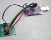
I have to spend hours to rebuild below project when I need to do a simple test:

Let's carefully recall our minds and list all the issues for the jumper wires:
1, Jumper wires are easy to lose connection after certain times of plugging in and out.
2, Jumper wires are NOT suitable for high speed
3, Jumper wires are NOT friendly for debugging, NOT friendly for signal testing with oscilloscope probes.
4, Jumper wires are good for very simple projects, but they become messy when more cables are added in.
5, Jumper wires are hard to set up when more than 10 wires have to be used
6, Jumper wires are fragile and have to be handled very carefully when moving a project setup from one place to another.
7, Jumper wires are tough to maintain the settings, especially need to be re-set up several weeks later.
8, Jumper wires are consumables, and you will find there are no cables available in your drawers after a certain time no matter how many you have bought, you have to borrow some wires from another project, which is carefully stored in your cabinet. This again makes you headache when you have to re-set up “another project” in the future.
9 Other issues, for example, the head pin of jumper wires accidentally touches a PCB and gets the PCB board spike.
So, is there any other option to overcome the shortages listed above? What alternatives are available for replacing jumper wires?
The answer was NO when I searched it over the internet.
As an electronic engineer, I thought this was quite a good point for me if I could design a board to fix most problems listed above and that's where my solution comes in—I've developed a new board called the "JumperLink."
What is a Jumperlink?
A Jumperlink is a board with a FPGA on and provides a configurable switch function for external connections.
A diagram will be much more useful than any words.
The basic idea comes from my experience using jumper wires. Any one wire will be connected to power or a signal. so I asked myself if I could make a connector with any pin that can be configured as a power output or signal input/output by software, then it is able to be used to connect most external devices. those external devices which are easy to purchase from online, such as from sparkfun or aliexpress etc.
As shown in the picture, Jumperlink has one FPGA in the middle and 20 pins on both left and right sides which is symmetrical in design. a multiplexer is added to each pin between FPGA and connectors, which makes each pin of the board able to be connected to 5V, 3.3V, signal and Ground. All signals are connected to a FPGA in which all of them are able to be configured from software. 3.3V and 5V are selected because they are the most common power in the embedded world.
this is the PCB I completed:
More details about Jumperlink
Jumperlink includes many useful features. Below is a summary of the key highlights:
1, Board size: 180 mm × 25.4 mm
2, Uses standard 2.54 mm pitch headers/connectors
3. Provides up to 20 pins on each side
4, Default connector configuration: female connector on the left, male header on the right
5, Any pin on the left side can be linked to any pin on the right side, and vice versa
6, USB Type-C connector provided:
Used to download configurations to the board.
Supplies 5V and 3.3V (via onboard DC-DC converter) to external devices.
7, One onboard button to enable or disable all links on both sides
8 One status LED for indication
9, Maximum bandwidth: up to 150 MHz per pin
10, ESD protection on each pin
11, Maximum current per pin: 150 mA, with a total current limit of 2 A (USB power limit)
12, Multiple Jumperlink boards can be used in parallel to increase the number of connector pins
13 Each pin can be configured with 7 options:
Hi-Z, 5V, 3.3V, GND, Input signal, Output signal, OD (Open-Drain) signal — mainly for I²C buses
Jumperlink is well suited for everyday applications, but it also has some limitations that are important to understand:
- 5V and VCC are output-only
- Each signal path includes approximately 1.8 Ω resistance existing in the internal multiplexer
- Maximum power output is limited by the USB port: 5V / 2A
- It supports digital signals only — analog signal switching is not supported
- When multiple boards are used in parallel, there is no communication or synchronization between boards
Before going deeper into the technical aspects, the priority is to first show you how to use Jumperlink.
How to use a Jumperlink?
To enable flexible link configuration, we’ve developed a dedicated PC software tool. Its main functions include:
1, Selecting the pin type
2, Creating links between two pins when they are configured as signals
3, Downloading the configure to the board;
4, Saving configurations as files on the PC, which can be reopened, edited, and re-downloaded to the board
5, Adding simple text descriptions for each pin for easy identification.
Below is the quick user guide:
1, Open the software tool
There are 40 units in total, labeled L1–L20 and R1–R20.
They represent the 20 connector pins on the left side and the 20 connector pins on the right side.
2. Select the pin options—such as 5V, 3.3V, ground, or a specific signal type—and connect the signals together according to your actual requirements.
The above configuration is equivalent to the one shown below—imagine two physical wires connected between L15 and R7, and L17 and R9. It would look like this:
3. Click Save to store the file in a local folder.
Click Build to generate the configuration bin file.
Click Upload to download the configuration bin file to the Jumperlink board when the USB cable is connected between the PC and the board.
An example
I would like to use a real-world example to demonstrate how Jumperlink can be used in a project.
Below is a simple project that I previously worked on.
It’s a simple setup: a Raspberry Pi I/O board connected to a TM1637 LED module. Four jumper wires are used to establish the connection.
The specific wiring diagram is shown below:
I chose GPIO20 and GPIO21 because they are located at the end of connector J8 on the Raspberry Pi board, making them easy to access and reconnect whenever needed.
However, if I want to use GPIO5 or GPIO6, for example, it becomes less convenient. Each time, I need to refer back to the pinout diagram and count the pins from 39 down to 31 several times to ensure the connections are correct.
By comparison, using Jumperlink makes the setup much easier. As shown below, I configured GPIO20 and GPIO21 in the Jumperlink application to replicate the same connections as the jumper wires. The detailed configuration is as follows:
No changes are required in the Raspberry Pi software, and the program runs as expected:
As shown, Jumperlink’s right-side connector is aligned with the lower section of the J8 connector on the I/O board (pins 21 to 40). This alignment makes it very easy to verify whether the connections are correct. Compared with using jumper wires—where you often need to count pin numbers repeatedly—the pin order is much easier to follow, as long as Jumperlink is always connected to the CM4 I/O board with bottom alignment.
With this setup, pins R1 to R20 correspond directly to pins 21 to 40 of J8. Users can also rename pins in the app for clarity. For example, R16 can be labeled as GPIO19, since R16 maps to pin 35 of J8.
Once R1 to R20 have been renamed and the configuration file is saved, users can duplicate and reuse it for future projects, as long as the setup is based on the J8 connector of the I/O board.
Now let’s look at how to connect the left-side connector.
The basic rule is that any four pins on the left side can be used for the TM1637 LED module. For example, you can connect L13, L15, L17, and L19 to the module.
Alternatively, the same four pins can be used with the module rotated 180°, depending on the physical orientation of the TM1637 board.
Extend boards
Some of you may have noticed that an extension board was used in the example above. The purpose of the extension board is to make Jumperlink more universal and adaptable to different connector types.
For example:
A male-to-male (head-to-head) pin connector allows Jumperlink to connect to devices with female headers.
A female-to-female extension board allows Jumperlink to connect to devices with male pin headers.
Extension options are also available for right-angle connectors, making it easier to accommodate different mechanical layouts.
Conclusion
As demonstrated in the examples above, Jumperlink significantly improves the way two modules are connected. It makes connections easier to set up, easier to maintain, and easier to share with others.
Since the project is still under development, any ideas, suggestions, questions, comments, or specific requirements are very welcome. Please feel free to leave a message on the blog. I will review them one by one and respond as soon as possible. Thank you.
Discussions
Become a Hackaday.io Member
Create an account to leave a comment. Already have an account? Log In.