 Paul McClay
Once upon a millennium past, AT&T tried to put protected virtual memory and preemptive multiprocessing on desktops. The world was not yet ready.
AT&T UNIX PC a.k.a. PC 7300 a.k.a. 3B1 a.k.a. (Convergent) S/50 a.k.a. S4 a.k.a. Safari 4
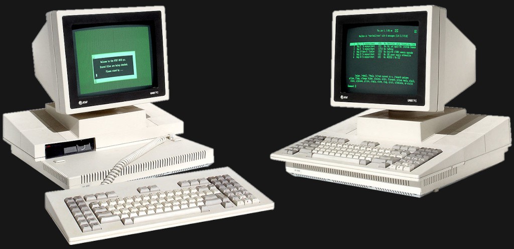
This is mostly about the AT&T UNIX PC Reference Manual and AT&T UNIX PC Service Manual. It's all the result of one guy's brief fit of "research" and shouldn't be trusted. For brevity I'm just going to say stuff like it's true. Caveat lector.
Reference Manual
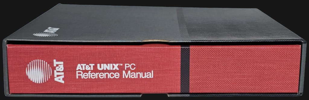
There are a few scans of the Reference Manual online. The most useful is https://web.archive.org/web/20260928201015/https://6reoquestions.s3.us-east-2.amazonaws.com/misc/UnixPC/UNIXPC_Ref_ocred.pdf. [2]
- OCR processed -- searchable
- complete -- i.e. all the same content as my real copy
- mostly in order -- i.e. mostly same order as my real copy except:
- appendices to the Reference Manual proper are at the end after all the extra stuff
- schematics in different order -- but order appears arbitrary so no matter
- the scan is good
- text is fine
- schematics are sufficiently legible for sane perusal
- insane fixation on minutia might warrant a real copy or better scan
- might be scanned from early copy
- title page is simple text instead of dressy color graphic card stock
- no evidence any updates to content regardless of date or packaging
- 488 pages (for quick differentiation from other scans)
- content by PDF page:
Reference Manual: 4 preface / ToC 14 Ch 1: System Features and Functions 38 Ch 2: Logic Board Theory of Operation 144 Ch 3: Diagnostics 174 Ch 4: Logic Board Test Procedures Reference Manual: schematics 228 video i.c. 232 DMA address i.c. 234 D-08-00222-00: "S4, CPU" [0.5MB as four banks of 64k-word with 256k/2MB option described] 262 D-08-00225-00: "S4, CPU P5 (1.0MB)" [as two banks of 256k-word) 288 D-08-00230-00: "S4, CPU" [um... see note 3] Reference Manual: appendices at end additional topics: 314 Floppy Tape Interface Theory of Operation 336 RAM-COMM Expansion Board 346 International Version Reference Manual Supplement 352 DOS-73 Technical Reference 382 Ethernet Expansion Board Theory of Operation 418 S4BUS - AT&T UNIX PC EXPANSION BUS SPECIFICATIONS Reference Manual: appendices 458 A - PAL Equations 472 B - Mnemonics 480 C - Expansion Memory Locations - for search:
- I don't know what AT&T calls this designator: 999-300-189IS [4]
- or this one: PE 1620-127 REF MAN
- Part number / "comcode": 845660117
- for credit:
- original scan http://www.unixpc.org/UNIXPC_Ref.pdf made 2/22/2006 by corey@lod.com
- OCR version generated and published by "Forgotten Machines" historian AJ at https://unixpc.blogspot.com/ -- AJ's contributions will come up again on this page
About the Schematics...
After reading way too much of this [see notes generally but do you really want to go there?], I have some questions and a conjecture.
The D-08-00225-00 drawings for "S4, CPU P5 (1.0MB)" appear to be the most "evolved" or latest state of the main board while the "D-08-00222-00" drawings -- one of two sets titled "S4, CPU" -- reflect something closer to early production hardware.
I wonder if (Convergent for) AT&T produced any boards that could not have been configured for and stuffed with any of the 0.5MB/1MB/2MB RAM options. Maybe early boards allowed only 0.5MB or 2MB not 1MB. If so, I wonder if any later boards that added support for 1MB also removed support for 0.5MB. If any did, then I wonder if all did.
The May 1985 Byte article includes:
Main Memory
512K bytes of dynamic RAM with parity bit on motherboard,
currently expandable to 2 megabytes via expansion boards;
machine's design allows for a maximum of 4 megabytes
...
Optional Hardware
512K-byte expansion card, $1195
One of the priced configurations includes "1 megabyte of memory (includes 512K-byie expansion card)"
That indicates that 256Kbit chips were not yet commercially advertisable but were allowed for by design. Given the non-availability of 256Kbit chips, it does not indicate whether or not 1MB on board was possible. The D-08-00222-00 drawings fit that scenario.
Did AT&T sell non-3B1 UNIX PCs with 2MB on the main board? 1MB?
A 1985 3B1 spec sheet (presumably published after Byte went to print for May) offers "1 MB or 2 MB expandable to 4 MB". Appendix C of the Reference Manual says the only way to 4MB is starting w/2MB (I.e. no 0.5+1.5+2), so the memory options parse as 1MB or (2MB expandable to 4MB). That doesn't directly say 1MB 3B1s had 1MB on the main board, but silence about including expansion/consuming a slot and stuff I think I know because something somewhere indicate the 1MB 3B1 option had 1MB on the main board like D-08-00225-00 drawings. Assuming AT&T didn't corner themselves into requiring different PCBs to stuff with 1MB or 2MB, that indicates a board that could have been stuffed with 1MB or 2MB, which is likely what the D-08-00230-00 drawings were trying to depict, per note 27 on the first & 18th sheets. It doesn't indicate whether or not later/3B1 boards could have been configured for and stuffed with 64Kbit chips to build 0.5MB UNIX PCs.
Would (Convergent for) AT&T have cornered themselves into requiring different PCBs to build UNIX PCs (7300s) vs 3B1s? I doubt, especially when it would have been easy to not do that.
Maybe early 7300 PCBs had no provision for stuffing with 1MB. That would seem odd since AT&T offered, or at least wrote sales copy for 3B1s within the first year, so that option had to have been in the works. Could it be that the 7300/UNIX PC got pretty far along in development as a 0.5MB/2MB concept (the -00222- drawings) until the cry from sales folk for a middle option got loud enough and the development press-to-market got quiet enough to give someone motive and opportunity to spot an easy way to make a 1MB option? Might a new 1MB-capable moboard have been the real reason "3B1" came through the new product pipeline instead of just a top cover & power supply upgrade? Anyone with an early 7300/UNIXPC care to scrutinize the board to see if it could have been jumpered for and stuffed with 1MB?
Maybe late 3B1 PCBs had no provision for stuffing with 0.5MB (64Kbit chips). Anyone have a late 3B1 to examine? Between the "P5" title and differences from the -00222- drawings, I suppose the -00225- drawings represent a late or final revision of the board. Were any non-3B1 UNIX PCs made with "P5" boards?
Anyhow, here's my conjecture:
At least some boards could have been configured for and stuffed with any of the three on-board memory configurations. Plausibly some early boards didn't support 1MB. Possibly the last boards gave up the 0.5MB option, but I doubt that.
The -00230- drawings include both 'note 27' re populating with 1MB or 2MB, and 'note 10' (and JR1 on sheet 18) re populating with 0.5MB or 2MB. If the -00230- drawings were believable, that would indicate intent to accommodate all RAM options. I think 'note 27' says pretty clearly that someone at some point thought there should be boards that accept both 1MB & 2MB.
In the -00225- drawings for a 1MB machine, which really means a machine with only two banks of RAM instead of four banks (of low or high density chips for 0.5MB or 2MB):
- the point is to show a minor modification to arrange RAM in two banks instead of four banks (of low or high density for 0.5MB or 2MB)
- schematic features related to populating four banks are simply omitted. Dunno why. For example, I doubt any board was made for 1MB that didn't have all the "NC" outputs from sheet 17 connected as usual to IC positions which simply remained unpopulated, and have all the wiring and open positions for the address MUXes deleted from sheet 18 (as described in note 27 of the -00230- drawings)
- sheet 17 includes JR6 in the LA1 line, and "LA2" labels on the +5V pull-up. I suspect both were minor goofs in adapting the drawing to add the 1MB (two banks) bits and delete the 0.5MB/2MB (four banks) bits. For weak corroboration: both features are absent from the -00230- drawing in which sheet 17 is drawn as for two banks only. There is no reason to disconnect LA1. I suspect the idea that got confused between drawing 1MB bits and erasing 0.5MB/2MB bits was to insert JR6 into the LA2 line and add the +5V pull-up as the other thing it could connect to.
- sheet 18 includes LA2 as an input, and inserts JR10 into that line. There would be no reason to disconnect LA2 in a two-bank-only (1MB) board. I suspect that 1MB-capable boards make MA20 available as the other thing that this jumper could select for the bit9 MUX input.
- With the possible exception of early non-3B1 boards, I suspect that all boards since the introduction of 1MB as an option have these jumper (and cuttable default trace?) options to select LA2 or pull-up as a bank-select input, and to select LA2 or MA20 as the "A" value for the 9th bit in bank address busses.
- sheet 18 also drops the option to configure for low-density RAM chips (0.5MB). However it does show a JR8 in the MA19 line. There would be no reason to disconnect MA19 in a high-density-only (1MB/2MB) board. I suspect JR8 is really JR1 between E1(MA19) & E2 as in the other two schematics, and that the E3(A11) option is still there. Later board revisions may very well have eliminated the default E3-E2 trace so that cutting it wouldn't be required for high-density RAM, but there would be no reason to retain any jumper in the MA19 connection unless A11 was still available as the other option.
So I think it's likely that the -00225- / "P5 (1.0 MB)" schematic artificially omits memory config options from the drawings that are actually available on P5 boards, and probably on any board that was or could have been populated with 1MB, and possibly on all production boards, or all but the earliest.
To "complete" the -00225- drawings by undoing over-focus on the 1MB configuration, I think it's likely that these changes would match real hardware:
- restore 'note 10' (sheet 1 for information)
- add 'note 27' from -00230- drawings -- as "note 30" after -00225- notes (sheet 1 for information)
- replace sheet 18 with sheet 18 from the -00230- drawings, editing 'note 27' to 'note 30' -- i.e. add note 10, note 27/"30", and JR1/E1-3 detail (shown with E2-E1 as preferred connection instead of E2-E3 as in -00222-)
- in sheet 18 retain JR10 and make MA20 available as the other jumpable option
- in sheet 17
- restore the LA2 connection as in -00222-
- move JR6 from LA1 to LA2
- make +5V (via 1KΩ) available as the other jumpable option
Service Manual
The Service Manual is also available online at: https://web.archive.org/web/20240609125007/https://6reoquestions.com/misc/S50/S50_Service_Manual.pdf
That's the straight-up AT&T UNIX™ PC Service Manual in a Convergent suit.
Outside:

Inside:

This might be news. At time of writing, I don't find any mention of an available scan of the Service Manual in the 3B1/UNIX-PC world.
AJ, who OCR'd the Reference Manual, posted a link to this scan in one of his relevant blogs: https://mightyframe.blogspot.com/2018/01/convergent-technologies-branded-model.html and further clarified in email "The buyer of the S/50 scanned the manual and shared it with me."
If you didn't already know: Convergent Technologies, Inc. designed and manufactured these machines for AT&T, and sold a few under their own name with nearly all of the AT&T branding intact under a very thin "S/50" veneer. Conversely, the AT&T Reference Manual includes clear "Convergent" branding on the schematics.
- the scan appears to be complete
- content matches the ToC...
- ...which matches a ToC reported from an AT&T manual
- content by PDF page:
7 preface / ToC 13 Ch 1: System Features and Functions [generally similar to Reference Manual] 37 Ch 2: Using the Diagnostic Test Procedures 75 Ch 3: Troubleshooting 93 Ch 4: Removing and Replacing Subassemblies 127 appendix A - Part Numbers for Field Replaceable Items 131 appendix B - Monitor Adjustments 133 appendix C- Expansion Memory Locations [duplicates Reference Manual] 143 Index - for search:
- I don't know what AT&T calls this designator: 582-602-030IS [4]
- or this one: ST-2129-16
- part number / "comcode": 845659697
- for credit:
"Forgotten Machines" historian AJ received the scan from an S/50 owner and shared a link in a blog post: https://mightyframe.blogspot.com/2018/01/convergent-technologies-branded-model.html
Notes
Notes, referenced by [square brackets], appear on the next "Page". Because this rabbit hole went deeper than HaD's max Page length.
Discussions
Become a Hackaday.io Member
Create an account to leave a comment. Already have an account? Log In.