 Torbjörn Lindholm
Disclaimer:
This review is sponsored by JLCPCB and the board was manufactured and shipped free of charge.
However, the contents of this review has not been doctored, monitored or otherwise influenced by them. That is, I'm not paid to make this review.
All parts of this review is honest and reflects only my perspective without any outside pressure.
Now, with the legal stuff out of the way, let's begin.
So I have been contacted by the people at JLCPCB, a printed circuit board (and related product) manufacturing company based in Shenzhen, China, about this review.
I, of course, said yes since I had a PCB I really wanted to have it manufactured. (guess what it is -- a little medallion)
I made the design in KiCad and generated the Gerber files (and drill files) based on their tutorial, which is on their page. (https://support.jlcpcb.com/article/44-how-to-export-kicad-pcb-to-gerber-files)
The first designs were not processed because the errors were caught during the auditing process:
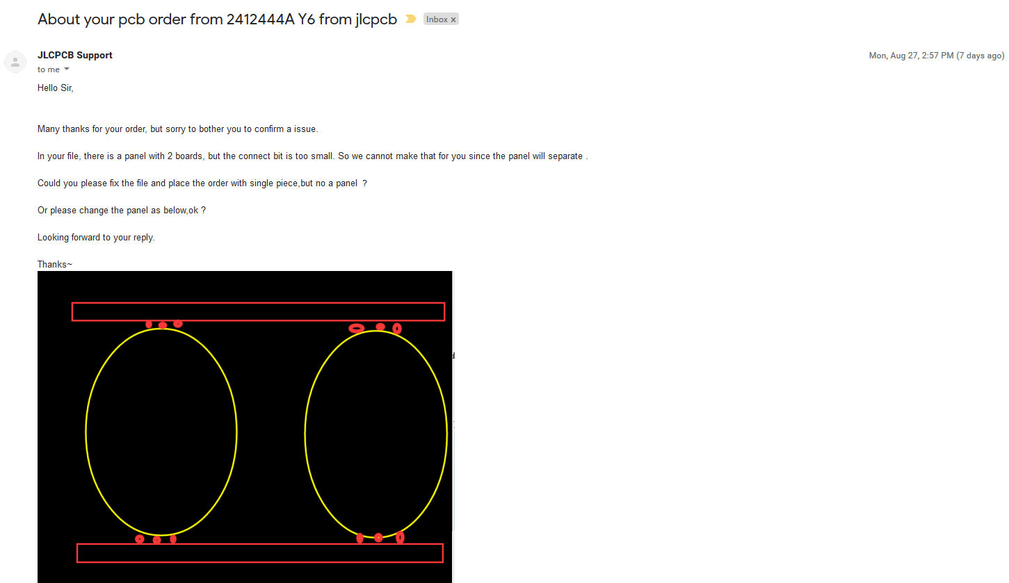
Their support representative was very kind and informative, and told me exactly what to do to have the design manufactured without problem.
I increased the bridge width and did what they suggested, and it was approved.
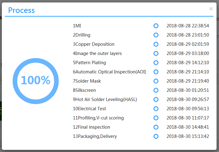
The page also has a progress meter which tells you what process is being done, which is handy. It's like watching a 3D model of yourself being printed on a 3D printer. Or seeing a CNC mill doing its job the first time.
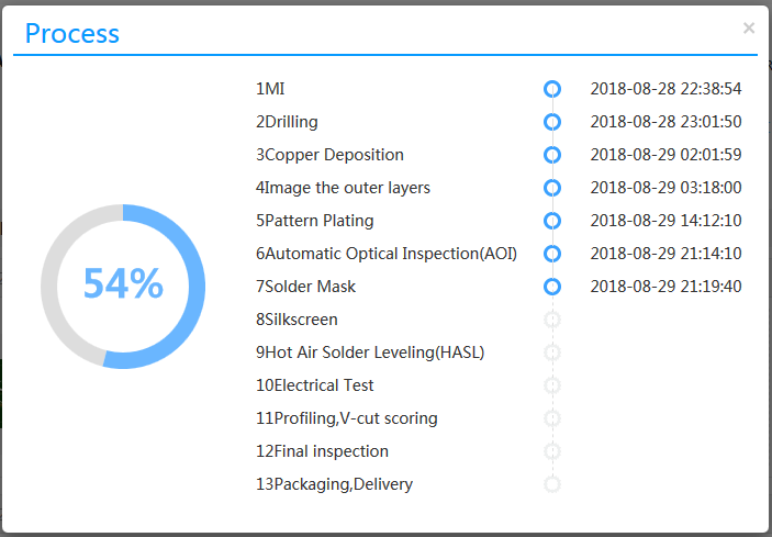 After a bit of dum-de-dum-ing and finger twiddling, the process finished.
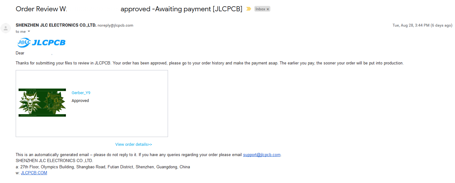
And after a bit of waiting (again), I receive a mail:
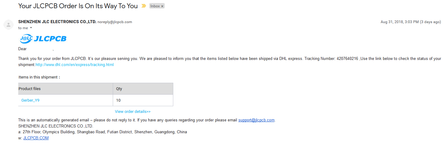
And the first thing that went through my mind was: YES! WHOOHOO!!!!
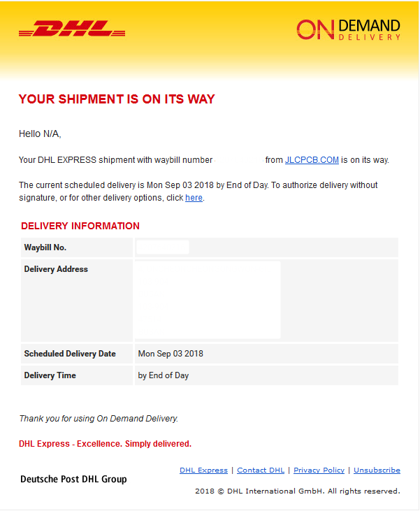
Then nearly immediately (in terms of business days) I get another email, this time from DHL.
(They provide some offers -- The green PCB is $2, and they have free shipping on first order. You can enjoy fast 3-day express shipping on your brand-new project!)
And after few days from that, I receive the boards in a nice package:
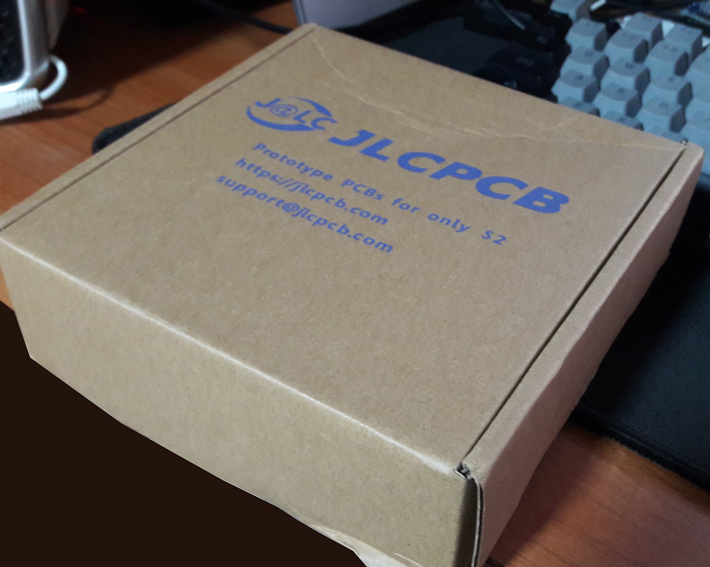
Inside was a double-wrapped package containing the finished PCBs, once inside the bubble mailer package and once in the vacuum-pack.
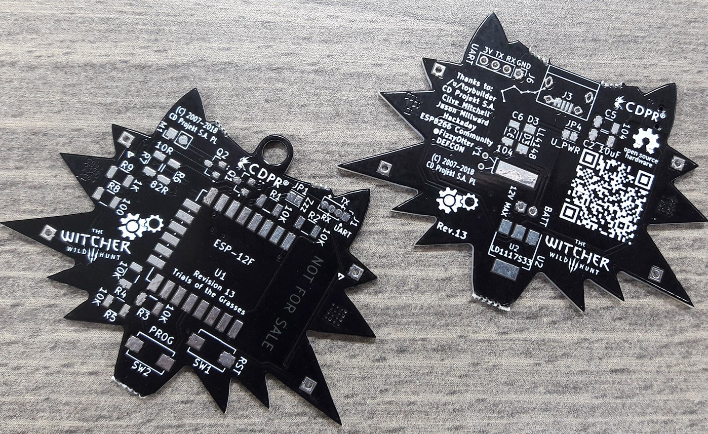
Here's the separated PCBs -- The quality is really really good. The bottom part looks messy because I didn't put enough holes there and it actually made it difficult to snap the board without breaking it in half or damaging it, so I had to basically saw it off.
I made a mistake with CH340G footprint, but it actually made it possible to show how accurate their PCB manufacturing process is:
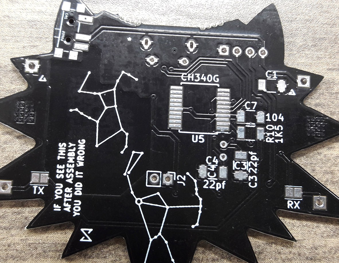
The footprint is SSOP-20 and it fits perfectly there. Of course, there is no SSOP-20 CH340G, so it was only there for testing.

Here I zoomed into the logo - the "Wild Hunt" text is about 0.8x1.0mm per letter.
Also here, I zoomed onto the one of the corners:
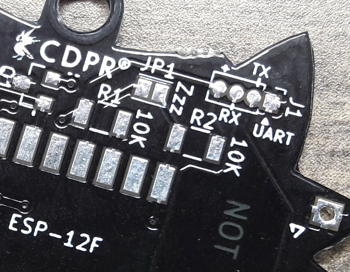
All the text is 0.8x1.5mm in size, and the pads are quite small at around the size of a sesame seed.
The lines are very sharp and they will actually warn you if it's beyond their capability (you can test this by using their Gerber viewer)
The board is very solid, too. This will certainly last for quite a while even in humid places.
I have yet to test the board (because the parts are not here), but I can say they take solder very well, they have no apparent manufacturing errors, the pads are exactly like what the Gerber file said it was, the spacing was dead-on, and the artwork resolution is phenomenal.
Super accurate double-layered board for $2?* That's some price you couldn't easily beat!
They also provide lots of thickness options, with 0.6~1.6mm boards provided with no additional cost. (0.4mm and 2.0mm boards will have some additional engineering fee)
You can also order a SMD solder paste stencil alongside your PCB order if you are gonna use reflow oven to quickly make many boards (for events such as DEFCON!)
You can also order electronic parts straight from their other shop (called LCSC) if you provide them with BoM. They will find the parts (if they have it in their catalogue) and ship it to you.
Use the code JLC6 on checkout to get a big discount -- $6 for the first order, no matter how large it is**!
So, the conclusion?
I'm very satisfied with the result, and for the price of $2* I'd say they are perfect for the prototyping purposes OR even commercial-grade projects!
I highly recommend JLCPCB for your projects!
* Only applicable to green soldermask option
** Read their ToS for more info
Discussions
Become a Hackaday.io Member
Create an account to leave a comment. Already have an account? Log In.
wow . Very good , It will be better , if your wolf is red ......
Are you sure? yes | no
FWIW they also charge an engineering fee for boards that are wider than 100mm, it seems. (I redid a board just because it bothered me). And $2 is fine, the cost of shipping makes it in the same range as oshpark for smaller boards. It starts becoming advantageous when boards are getting to the size of a Raspberry Pi or above.
Are you sure? yes | no
That is true; They charge extra for boards larger than 100mm in any axis.
Are you sure? yes | no