-
GPL Compliance Issues in Z80-MBC3
05/22/2026 at 04:05 • 0 commentsA Retro DIY Machine With a Modern Licensing Problem
By David Collins
License note: This document discusses and quotes evidence from GPLv3-covered Z80-MBC2 material. The evidence archive includes the full GPLv3 text in LICENSE and repository-specific attribution notes in NOTICE.md.
Provenance note: The developer statement cited in the evidence archive is preserved at:
https://github.com/lindoran/Z80_MBC3_GPL_VIOLATION/EVIDENCE/provenance/Willem_Vrieze_Facebook_20230103.pngA detailed repository containing all the information below including cryptographic hashes is below:
https://github.com/lindoran/Z80_MBC3_GPL_VIOLATION/
I don't usually write pieces like this. Most of the time I'm focused on fun hobbyist projects; things I'm building myself or trying out and sharing with all of you. But this issue hits close to home. The Z80-MBC3 has been around for a while now, and judging by the activity in its Facebook group, it's become pretty popular.
What matters to me, beyond the joy of building these little computers, is the trust that holds this community together. Open-source projects only thrive when that trust is respected, protected, and passed on so future hobbyists can enjoy the same sense of discovery we do today.
I'm certain I don't need to dive too deeply into what the GPL is; with Vizio, Bambu Lab, and others in the news lately, it's become a familiar topic in the circles we all follow. Most of the time, these stories involve large companies with established brands and millions of dollars tied up in legal battles.
But what happens when a hobbyist runs into the same problem? Where does a small developer turn when someone blatantly disregards the trust that keeps this community alive, all for personal gain or borrowed accolades?
In the end, it often falls to us in the retro community; to speak up, enforce the standards we care about, and vote with our voices and our wallets. And today, that's exactly what we're going to do.
I tried to provide as much information as I have, but if you want to skip to just the facts behind the actual compliance issue go ahead and skip to the section "Where we are now" if you are already caught up, or if you actually were around in the Z80-MBC2 group in 2021 you probably would want to start there.
What is the Z80-MBC2?
Where do we start? Best to start from the beginning with the original: The Z80-MBC2 is a computer produced by Just4Fun (Fabio Defabis) for free — on the internet for anybody to build and make. Originally based off of the Z80-MBC dubbed the $4 Z80 computer (MBC for mobile, breadboard computer). A small computer that uses an ATmega32A as an IO controller that can stage the RAM and interface the Z80 at speed using a simple easy to follow wait/grant architecture. The Z80-MBC2 took this design further and produced a kit computer and the basis for several other computers all which share its form factor. This was immensely popular and beloved. Eventually, Fabio went on to produce several more designs, with similar chips such as the NEC V20 and the Motorola 68008. Simply, just for the fun of it. All of Fabio's projects are open source, and free for anybody to download and try out including the board fabrication details and schematics.
Much of the community activity around this computer and the whole family of MBC designs took place on Facebook. At the height of the 2020 coronavirus pandemic, the Z80-MBC2 Facebook group became the center of it all. Countless builds were completed during that time, with users helping each other, sharing fixes, and contributing enhancements. Some of the most impressive work came out of that collaboration, including support for Fuzix, the POSIX-based UNIX-like environment for the Z80. The atmosphere was one of camaraderie, generosity, and genuine enthusiasm.
The period from 2019 through late 2021 was very formative for me as a maker, and I owe a lot of what...
Read more -
The Curious Case of the VZ200 Chip-set (Part 2)
12/15/2025 at 04:00 • 0 commentsWhat’s next?
We’re still chugging along on the VZ200 clone, building it out as a set of RC39‑style modules on a back plane, all as part of our open‑hardware project with PCBWay. A bunch of the boards are already up and running, and the machine now boots into a serial ROM monitor where I can poke at RAM and ROM, its early days however things are progressing nicely!
![]()
RC39 Backplane with VDG Board installed
But then I hit a snag with the display memory circuit.So this is the story of what happens when you take a simplified 1980s chip set and try to squeeze it into a GAL to save board space and a bit of cash. Let’s walk through what it actually takes to get this tiny display module to read and write its RAM chip the way it’s supposed to.
The VDG problem:Last time we talked about how the 6847 expects bus arbitration pulses to clear its address strobes off the bus so the CPU can write to memory. We went over how this creates snow artifacts as the 6847 tri-states the address bus outputs. We also went over how the timing of the specific logic inside the circuit is paramount to making sure the 6847 is off the bus so that the CPU can make an uncontested write operation.
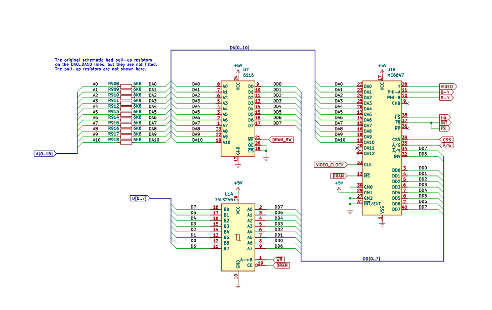
The Schematic:But what if we don’t want to use LS logic from the 1970s to accomplish our video module? Let’s go over the video circuit in detail by looking at the schematic.
![]()
rweather schematic snip linked to github We see that the data bus is separated by a bus transceiver, from the 6847 (VDG – Video Display Generator) and RAM chip data pins. Going over what we know about the VDG from the last time, it has to strobe through all of the addresses on the RAM chip and build a raster 60 times a second no matter what. That's because the 6847 isn’t really a video display processor, it’s a finite state machine (FSM) with selectable states. Some of these states are selected by data pins, and some are selected by separate control signals from an external register typically (in our design they are). The VDG really only knows how to run a few tight loops: scan the RAM and display in text mode, scan the RAM and display in graphics mode and so forth. These “states” in a fixed path tight loop are what makes the VDG a state machine and not truly a dedicated video co-processor. Essentially, it scans the RAM really fast and pushes out a bit stream, as well as create all of the relevant sync and color information pulses over and over; forever, unless you change the state or interrupt them. Think of it as an elevated version of the “TV Typewriter” but with much of that circuit already built into the box, including the character ROM!
The Crux of the Problem:So we have established, essentially, the circuit has to keep the data bus and the address bus clear of contention whenever the 6847 needs to push out a frame to the display. The circuit does this by separating the address bus with a bank of resistors, and the data bus with a bus transceiver. When the /DRAM signal is generated in the chip set the address bus on the VDG cuts out, the data bus aligns with correct directionality, and the RAM chip is selected. Ultimately this creates snow because the CPU does not know when the VDG is on the RAM it only knows it can knock the VDG off the RAM by writing to or reading from it. This works well, it’s simple and cheap but obviously the issues are:
- Timing is tied to the logic family, and the specific construction requiring multiple chips
- Even though the CPU and the VDG are clocked by the same clock, they are not synchronous. The Address decode, write and read cycles of the Z80 prevent the two devices from truly being able to avoid contending with one-another.
- The VDG is knocked off the bus on every single write and read to the display memory, this “second fiddle” bus positioning means lots of artifacts.
- Artifacts are annoying and they can ruin user experience.
- The decode circuits cascade decoder chips, which leads to large ...
-
The curious case of the VZ-200 Chipset (Part 1)
11/26/2025 at 22:25 • 0 commentsIn this Series
We're going to build a replica VZ200, a very interesting off the shelf home computer, done on the cheap, but also quite popular in the markets that it dominated. In this part we will go over the chipset at its heart and try to explain how it's one of the cleverest little minimal designs of its time.
We will work with PCBWay (our sponsor) to build a brand-new backplane system all on cheap 100x100 or smaller PCB's just large enough for the task at hand and were going to do it all up open source, so you can hack on it to your hearts content and maybe make your own!
So come along with me as we explore the chip set of the VZ200, and the cheap computer that took the hearts of many young programmers. It should be a very interesting prospect indeed, and in the end hopefully we get a working computer to show for it.
The Basics
The VZ200 is a Hong Kong based VTECH (then Video Technologies) designed home computer. Produced in 1983 and based around the venerable Z80 CPU, and curiously the 6800 family IC the 6847 VDG (of Tandy CoCo fame). The computer's clock is operating at the NTSC color burst frequency, approximately 3.5795 Mhz. This computer was a first for a lot of kids in the eighties in places like China, Australia and Germany. NTSC versions did exist but the majority of the machines are PAL based (a fantastic story but not why we are here today.)

VZ200 image by way of wiki commons The computer normally outputs in PAL, though NTSC versions do exist. The chrominance and PAL line timings are generated by way of a daughter card, whose schematics have been redrawn by this clever user on GitHub. Video oddities aside, the scope today is simply to go over the 3-chip chip set, because like so many costs reduced computers of the day, it really was able to squeeze a ton of functionality out of such a low chip count.
The Design goals (squeezing blood from stone):
The VZ-200 uses 3 ICs to do all of the address selection and decode, 2 multiplexers (74LS138 and 74LS139) and a Quad OR (74LS32) . It also manages to control the bus arbitration for the VDG, simply as a side effect of fan out. The logic is all standard LS type logic so we can fairly well guess the propagation delay from the data sheets. Since the clock speed of our Z80 is known (approx.. 3.5795Mhz), we can calculate the T≈279.4nS. If we look at the actual logic design we can then simply calculate the timing delays for all of the select lines by doing some simple arithmetic.
We have good schematics for the VZ200, so we don't have to guess how they are all connected. for simplicity of this demonstration I took the liberty of building just the decode section in H. Neemans Digital
![]()
The chip set had to do five things ascertained by simply looking at the outputs:
- Control a number of 2K SRAM chips
- Control a number or 8K ROM chips
- Time High-Z logic for the VDG address lines
- Control a memory mapped IO range
- be cheap.
It is strange on a CPU that has a dedicated IO port instruction would have anything in the way of Memory Mapped IO. IO ports make accessing devices on the bus simple for the CPU but they can also add complexity to the selection logic. It is odd, but also pragmatic.
Z80 Cycles:
Cycle type MREQ RD WR M1 IORQ IN (I/O read) 1 0 1 1 0 OUT (I/O write) 1 1 0 1 0 Interrupt acknowledge 1 0 1 0 0 Opcode fetch (memory) 0 0 1 0 1 Memory reads 0 0 1 1 1 Memory writes 0 1 0 1 1 Bus idle / no cycle 1 1 1 1 1 IO selection on the Z80 happens when the CPU uses the OUT or IN instructions (mostly, but we will only go into that use case here). When this happens, /IORQ goes low, and /RD or /WR goes low as well. There's also another reason /IORQ goes low; that's during an interrupt acknowledge, however in that case M1 goes low. So,...
Read more -
New DC-DC Circuit for the 48k Speccy
06/30/2024 at 04:59 • 0 comments
Just before applying the DC-DC mods for the original circuit I received this 48K spectrum from a friend, in a mostly working state. It needed to have the membrane replaced as well as one of the 32K ram chips. Through the process of rework the DC-DC converter circuit began to fail. I believe as a result of being run at a high level for a long period of time, from an unregulated 9v supply that may have drifted slightly.
On initial inspection, I determined the 4116's must have failed as TR4 / TR5 kept blowing. I replaced them (t4 and t5) and removed the ram chips, to no avail as the transistors kept failing even with the ram chips removed. The next on the list to check was all the capacitors, I verified none were open or dead short with good ESR values ( all electrolytic were replaced first thing - and the board worked for a few hours at least). I suspected the coil was bad. At this point I started to deep dive into the circuit and read through two separate circuit descriptions trying to determine:
- why this circuit fails so much.
- why this was the most modified part of the circuit throughout the revisions.
- can this be improved uppon.
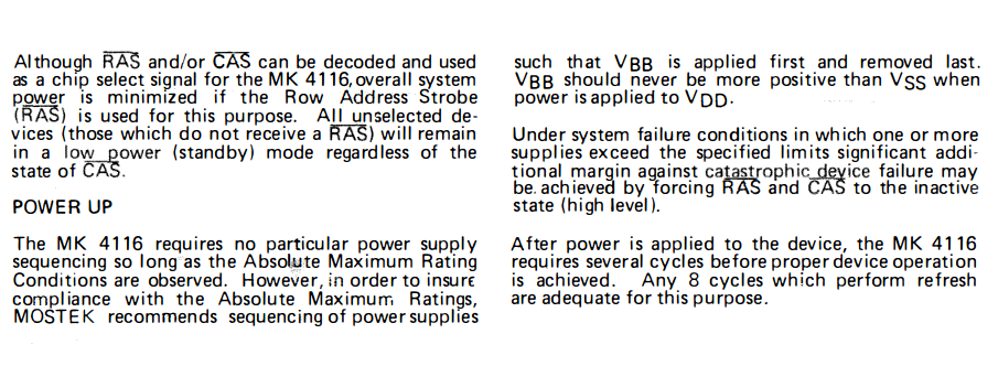
I asked my father, who was an EE from the 60's all the way to the 90's to take a look at the inverter / DC-DC circuits across the several revisions as he's vastly better at looking at analog circuits than I am. Together we determined that the DC-DC mods specifically address regulation and clamping issues in the previous versions of the circuit. While these improve supply output and manage transient voltages which feed sensitive ram chips it does not address what is conspicuously missing from ALL revisions of the 48k DC-DC circuit; 4116 bring up timing.
The 4116's and by in large the transistors inside the DC-DC circuit fail because the supply does not adhere to this note in the 4116 Datasheet:
![]()
Simply put - There is no timing mechanism beyond the R/C delay inside the circuit itself, which grants exclusively that VBB (-5v) is applied first, and removed last. Furthermore, when power is removed to turn off the system if the ground path is eliminated by disconnecting the cord completely or isolating the ground line in an improperly wired switch. There is no way to assure any sort of state on power down.
So - specifically when the 4116's fail, and they usually will, the DC-DC circuit is often damaged by an over current condition on the digital 12v rail.
So how did I improve upon the design:Back in the 80's the most commonly used dc power supply was an unregulated 9v center negative power supply. Specifically because of this utility its obvious to me that that is the reason that iconically thrifty Sir Clive and his engineers chose this to be the supply they were to use. Moreover - not wanting to spend any amount on a switch for every unit allowed them to cut the prices even further to save Sinclair millions, by simply having the public unplug the thing or turn the switch off at the wall socket. What was needed was a minimal, cheep and dirty power circuit to create the multiple rails required for the computer and not break the bank. I think they did the best they could with the limits they had, and specifically the computers worked well enough in the day for this oversight to not matter nearly as much as it does today.
Today, we have commonplace, high quality 12V regulated power supplies that run cool and efficient and don't really break the bank. I decided to remove the DC-DC circuit in my issue 3, and use an external regulated center negative 12v power supply to power the whole computer.
This has several advantages:
- The supply is more efficient - we no longer have to "boost convert" a 12v rail using a charge pump and inverter. This reduces losses to multiple conversions going from 9v - > +5V -> +12v & -5v
- The supply is cooler - the LM7805 linear positive voltage regulator gets...
-
HB63C09 Mezzanine Connection
01/21/2024 at 02:31 • 0 commentsThe mezzanine, your gateway to off board IO
Going over the memory map from the REV3 board, the astute will notice the entire IO range selects the AVR request grant logic. This poses an issue for off board requests from the mezzanine connection. To resolve this, the XSIN (transceiver inhibit) signal is utilized. XSIN is a active high signal (for now) that cuts off the bus transceiver output enable pin. This in effect leaves the bus available to the mezzanine connection:
![]()
When the loop starts inside the firmware the AVR (an ATMEGA32E micro controller) is just poling for IO requests. When it catches one, the MRDY state is already asserted on the CPU and the buses and the E and Q pulses stop in the state that they were in. This includes the data bus, r//w line and the address bus (along with all the other control signals as well). Immediately following this, it reads the XSIN line and determines if it is high. If so the IOGNT_ signal is immediately sent to the request/grant circuit and the read / write cycle can continue. This does have the disadvantage of added delay and a momentary clock stretch on every IO request, however it is very short, only a few cycles of the system clock. This was a needed trade of to keep the selection logic as simple as possible without expanding to a higher chip count.
In order to use the mezzanine expansion connector, the IO request logic must be replicated on the expansion. The IO request must also be assigned to an unused address in the IO range (for example, any address in A010-AFFF). The selection signal must be active high and linked to the XSIN line, which means that a standard address decoder must either have active high outputs or be inverted before using the signal. The XSIN pin is an input on the AVR, and it is pulled low by a 10k resistor. Only one output on the expansion should select this pin, because the logic on this line is push pull and multiple signals driving the pin high could cause a short circuit. During reset the AVR pulls this line high to zero the bank register. Currently I can not test the mezzanine until I resolve the potential short circuit. This is likely to change to simply having the reset pin for the register driven by RES (inverted RES_, which is generated by the reset circuit) but it was not high on the list of things to work out in this board revision, and so it was omitted. I am also considering changing the functionality of the pin XSIN to active low, by building out logic. Since the actual scope of the signal is for only one device it makes better sense to not make this a priority over other things which could potentially take more board space. The advantage to this is all of the signals going into XSIN could be open collector outputs and this would drastically increase the usefulness of the signal in a multi-slot expansion set up, if for instance somebody were to build a breakout with multiple slots.
If you'd like to learn more about the HB63C09M follow this link to the main project page.
-
7404/14 - Not all inverters are the same.
10/28/2023 at 04:21 • 0 commentsThe Problem:
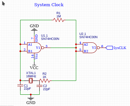
While debugging the HB6309 PCB REV1 I wanted to build a very stable oscillator I could drive the CPU and the Arduino with, I knocked together my standby: 1/2 of a 74HC00 and a 1K resistor and crystal with fairly mediocre results:
![]()
![]()
![]()
This is actually a very popular oscillator with hobbyists, and if were totally honest it works 90% of the time with no issues for the kinds of projects that we tend to gravitate towards. Even Grant Searle himself, uses the design in at least one of his Z80 builds. The biggest problem with this design (as you will see), is the inverter, a buffered NAND Gate, while its logical output is the same - its switching characteristics and internal circuitry are VERY different.
Before we get started, a gentle reminder to readers not familiar with my content. I am a hobbyist, and not a EE. I do have a very strong background in Civil Engineering in the telecommunications field, so if some of my examples or explanations are wrong - feel free to correct me! (we are all here to learn)
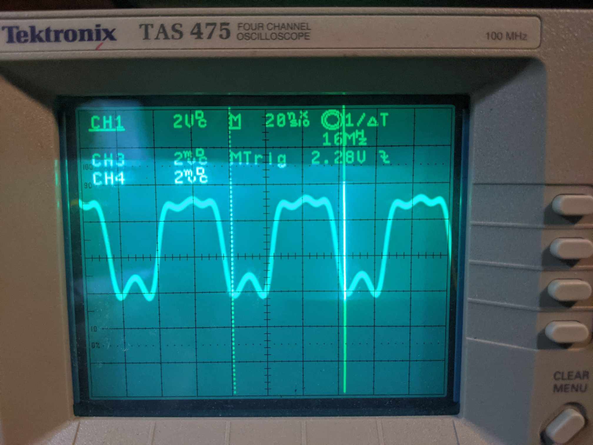
The issue:![]()
The internals of the 74HC00, we see the buffered inputs, while insuring proper logical signal triggering, actually dampen the analog properties of the circuit. Additionally clamping diodes on the input (and output) of the inverter may play a roll as well, though certainly not nearly as much as introducing buffers to the circuit:
![]()
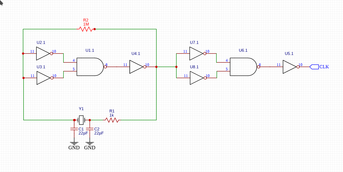
Just looking at the expanded circuit, you can see this is not even approaching a proper Pierce Oscillator. The root cause of the ringing are almost certain due to The first stage - to understand this better, lets look at a few different buffered inverters hooked up with a much better circuit recommended by Olin Lathrop on stack exchange
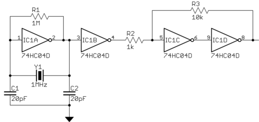
![]()
This circuit is considerably more suited to producing a very defined square wave. The first two buffers trigger the initial oscillation using a 1M Ohm resistor hooked in parallel. We see a sine wave (more or less, more on that in a second) on the input of 1A. A second inverter (1B) takes the trapezoidal output and cleans it up further. The second stage is a Schmidt Trigger, which introduces Hysteresis into the circuit, the first gate acts as sort of an amp to the second gate which drives the triangle wave produced by the first into a serviceable Square wave. Why not use just Schmidt triggers then?
Essentially, the first inverter is a linear amplifier - we know this because the 1M Ohm resistor from the input to the output acts as a bias to the input of the gate. This amplifier takes the relatively low sine wave output of the crystal, and turns it into a 5v PtP ish square wave. A Schmidt trigger is highly non linear (the whole point is to make the signals snap to the rails as happens in the second stage of the circuit), this is wonderful for generating a cleaner square wave than produced by 1B, but not so good as a linear amp.
I got curious so I built the circuit with a 74HC14:
![]()
This is the input of the first gate, see how the signal here is very non-linear, also note the fringing around the edges; on a digital scope this would be rolling like crazy as the time base changes, additionally the amplitude fluctuates as well -- this would be a wonderful circuit to analyze on a spectrum analyzer (unfortunately for me I only have access to that at work, and certainly not in a format I can probe a simple circuit I built at home)
The output IS technically a VERY defined square wave, but the time base is severely effected by the multiple triggers, interfering as the time base shifts:
![]()
Then I tried the 74HC04:
I kind of knew the results would be fairly similar to the simple 1/2 NAND solution:
![]()
Basically - this is the same though the multiple inverters pronounce the ringing on the High level base instead of the low level base. (this is also with a small value approx 33 Ohm dampening resistor on the output...
Read more -
ZX-81 Restoration news:
03/13/2023 at 17:00 • 0 commentsI moved development of the ZX-81 off the pages updates and to it's own Hack-a-Day project here : https://hackaday.io/project/189795-hbkd-81 if any body was following this space for updates on the restoration they are there :)
-
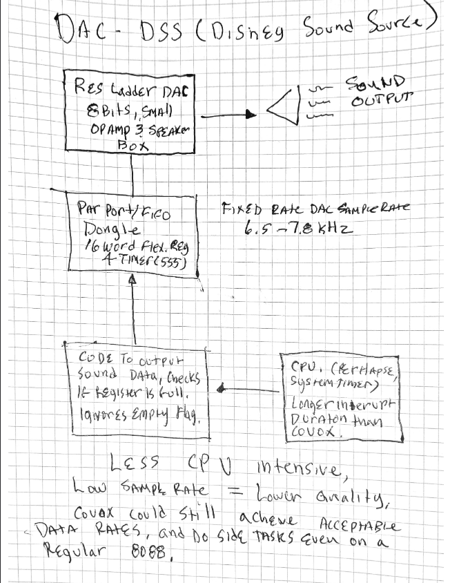
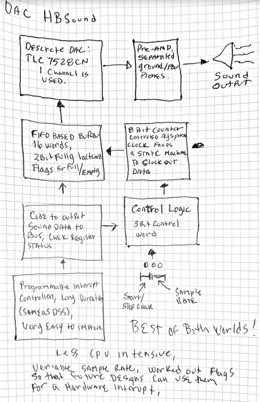
HBSound Block diagrams from my lab notebook
01/30/2023 at 04:13 • 0 commentsHere's some block diagrams for the HBSound project I pulled from my notebook:
I'll link the next ZX-81 blog here if you are wanting to skip to the next segment when that comes, right now waiting on a replacement modern ULA to be delivered from New Zealand. Hope to have more updates on that soon but for now enjoy my sloppy handwriting
![]()
![]()
![]()
-
Interesting Fail Mode, finding noise and isolating the issues.
01/18/2023 at 04:24 • 2 comments![]()
Success! well sort of:
Initial false start. I was able to get a 'K' Prompt to load, but with astoundingly bad ghosting. I went to work checking for the common things. --- ingress from cracked traces or loose connections the usual analog-ish type stuff. In Broadband when we have ghosting in a analog signal, we look for an impedance mismatch base band is not much different.
I checked with the scope and found there was very irregular reflections which got slightly better if I probed the reference clock circuit. I figured this was more about the probes veritable capacitor of a few pF then the huge resistor in my x10 probe. Checking for other obvious signs of a crack I decided to just slide the ULA from its socket slightly and re-seat it. This had little to no effect and I ran into some more issues with resets and starting up properly.
Checked a few more things and found that the !OE line on the ram upgrade was not connected but bent out. A quick google search found the specific mod being done here and I sorted the issue by grounding the pin (in this design only one of the enable lines are needed).
I flipped the board over and checked the pads under the ULA and found a few of them were not soldered very solidly so i re flowed a few of the pads. When i pulled back my iron from the third pad I started to uncover the problem --- the pins were coming loose from the socket above!
![]()
I removed the big chips from the board and found that most of the larger chip sockets were completely corroded . I don't have very sophisticated de soldering equipment, a manual pump, temperature controlled soldering iron and a good amount of solder wick. The easiest way of going about careful chip removal in a board this old without an automatic de soldering pump is to cut up the sockets and pull them out 2 or 3 pins at a time. This sounds time consuming but its actually quite efficient and probably only took about 15 minutes to remove all 3 sockets. Since I had the mask ROM and the CPU out, I replaced both with newer parts -- CMOS Z80, and a 16K 120nS EPROM. The Mod for the EPROM was fairly trivial, I just bent out the pins that did not line up and manually routed them which amounts to only 3 of the pins.
![]() I ended up cracking a trace replacing this socket for the Mask ROM. I ran a wire on the back side to the next point in the design (on of the bus arbitration resistors):
I ended up cracking a trace replacing this socket for the Mask ROM. I ran a wire on the back side to the next point in the design (on of the bus arbitration resistors):![]() After I replaced the broken trace I plugged everything back in, plugged in the computer and immediately ... got no picture... Its a 40 year old machine with aging corroded parts I have to be realistic and so I half expected this. This lead me down a number of avenues, I wound up toning out all of the traces using the schematics, and replacing the RAM expansion after discovering it was causing some of the lower address lines to stay low.
After I replaced the broken trace I plugged everything back in, plugged in the computer and immediately ... got no picture... Its a 40 year old machine with aging corroded parts I have to be realistic and so I half expected this. This lead me down a number of avenues, I wound up toning out all of the traces using the schematics, and replacing the RAM expansion after discovering it was causing some of the lower address lines to stay low. ![]()
SO... The saga continues.
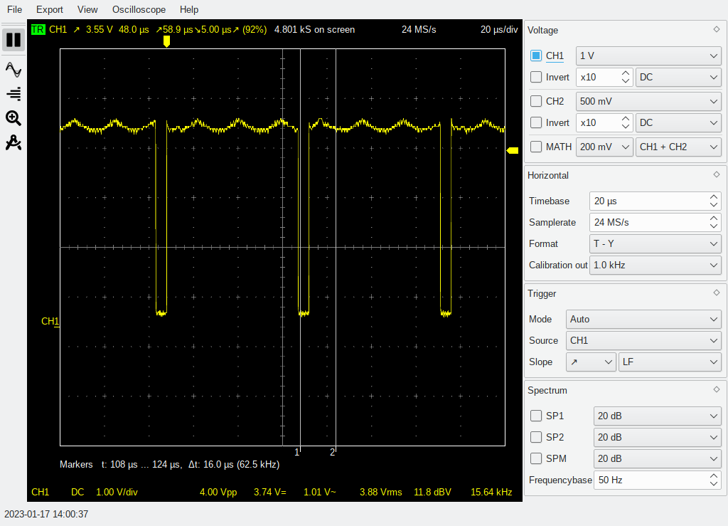
I went back to basics, Started probing some of the lines coming from the ULA, determined I was getting a sync signal but it looked very noisy:
![]()
So the amplitude should not shift like that, and though you cant tell because this is a still it does, roll across the top as well. - - it should be fairly flat. The line data is there (you can't see it in this screenshot.) and I pulled the time base out so you can see it. This looks like an oscillation, the clock for the CPU, the line clock and the sync are all made inside the ULA.
A new approach (Lets remove the DC Offset):
We have a sync but its very bad, so bad in fact that the TV can not see it as it just looks like DC voltage levels -- the best way to trouble shoot the issue at this point is to try to get the TV to display "something". I pulled the back porch mod; and built the simplest composite mod (from byte delight ~ image is linked:
after constructing the mod as designed - I added a 300uF or so electrolytic capacitor (to remove...
Read more -
ZX-81 Restoration Video Modification
01/11/2023 at 03:42 • 0 comments![]()
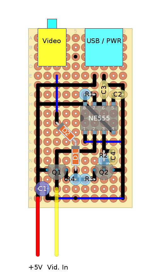
So while still waiting for HBSound's Prototyping sponsor, PCBWay, to finish up and ship off the prototypes for that project. I did have some time to work on the ZX81 Restoration. I am still working through the best way to clean up the corrosion without further damaging the silk screen, but I did have time to start thinking out soldering the video modification. Since the board came ceaseless, and without a number of it's connectors and modulator can enclosure. This afforded me the opportunity to build out the existing board the way I want it. And since I am building a custom wedge case enclosure to hold this thing; that is the plan anyway. I decided the best course of action was to solder two header pins in place of the can mounts and build up Ziggurat communications video 555 Mod to add back the back porch that's missing from the video signal. I cut a piece of perf board to fit across the two pins and went to work on modifying Ziggurat's strip board layout to work on perf board. This also allowed for re-positioned power and video connections. As I am building a new enclosure I moved the connectors 90 degrees to the back of the case to clean up the wedge esthetic so it matches the rest of my micros. If anybody has the slightest clue as to why Sir Clive decided to mount them on the side, instead of around the back shoot me a line, this has always mystified me.
The new layout:![]()
As you can see I didn't picture wiring through the connectors on my layout. I am still trying to figure out the best way to lay out the connections. I will also most likely run a larger gauge wire down the side ground rail directly from the back side of the USB connector to one of the larger power traces on the PCB since back feeding the full current of the power supply from the can input is most likely not the best Idea. If there is any interest to the DIYLC files I can provide them at request, though the circuit and diagram are easy enough to follow from the pictures provided. In keeping with the "volume of one" design rule I set for myself on this project, I will not likely do a layout for a PCB since I don't think its likely others will want my specific customization. Perhaps if I get closer to the case build, if there is interest I would reconsider, for now we will see.
BOM:
I used the exact same BOM from the Ziggerat board which i will replicate here (the source document gives permission with accreditation to Ziggerat ind.):
Resistors
R1, R2 10 kΩ
R3 68 Ω
R4 56 Ω
All 0.25 W, 1% metal film.Capacitors
C1 22 μF radial electrolytic, 16 V (or higher rating).
C2 10 nF ceramic disc.
C3 820 pF ceramic disc.
C4 82 pF ceramic disc.
Semiconductors
D1, D2 1N4148
Q1, Q2 PN2222
U1 NE555My additions:
18x10 Perf Board
USB B type connector
2 conductor easy to mount Video connector of your choice
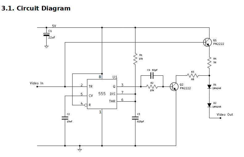
And while were at it the schematic:
(the source document gives permission with accreditation to Ziggerat Ind.)
![]()
The source document gives a very good description of the circuit function, so its not really needed to do a full work up here but if your are interested Oli's Old stuff does a fantastic job explaining the options, and Grant Serle has this resource on the ZX80, as well as this on the ZX81. Ziggerat industries Web Site is the original source for the modification (under misc).
Up next:
Up next is building and testing the circuit, as well as fitting it. I still have to do something about about the top board HASL; I may do some high resolution shots and ask around to see if it is problematic For now I cleaned up the stuff under the can ground plane as the video mod will be soldered in place on top of it and accessing later will be a different kind of hassle ;-).
If you have liked this please feel free to share, comment and check out my other projects here on hackaday.io. I usually have one major project going on and a few...
Read more -
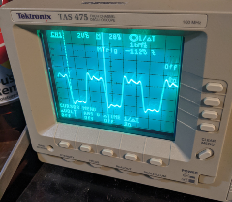
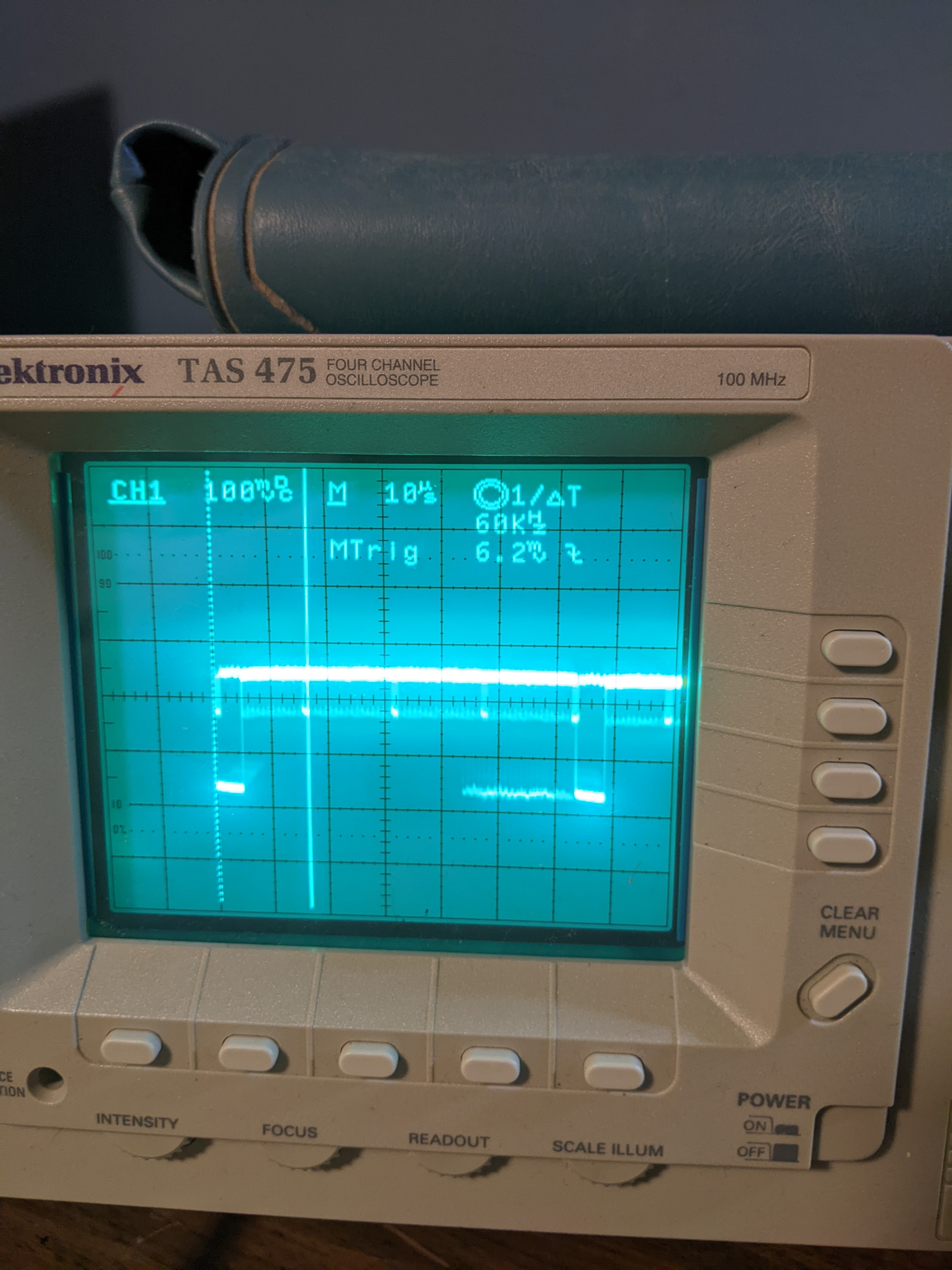
ZX-81 Progress / NTSC ULA Output
12/24/2022 at 17:53 • 0 commentsContinuing from my last post, I had some time waiting on parts to finish the analog prototype testing for HBSound so I set up the new scope and ...
It lives:
![]()
I like to think about the video output as the consciousness of these old home computers. Generally speaking enough of the gears need to be spinning to make this output correct (memory, clock ocilator, CPU and reset). It's also important that it shows line data being sent as this further improves chances we have a working computer.
The scan looks good but does verify the 'back porch' signal is missing.
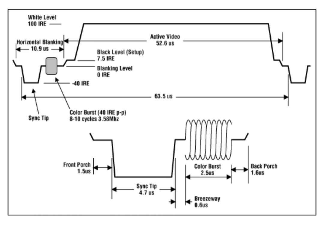
Here's an example of a properly formed scan for NTSC the example is with color burst so you can ignore that bit for the ZX-81 we're working on here:
![]()
(Graphics stolen from this excellent resource https://www.analog.com/en/technical-articles/basics-of-analog-video.html)
What we do have is a horizontal blanking pulse that sits at about 1v. This is indictive of some of the late release ULA's which do not actually generate a complete blanking pulse. This is probably fine for a crt displaying modulated RF. Today we need an appropriate back porch signal to make sure the black levels (among other things) display properly on a lcd. For this I will need to build up a small PCB with a 555 timer and some transistors to amplify the signal and ad back the back porch so it will properly display on a lcd.
![]()
I also took the time to clear out all of the needed points of solder and put a 'zero' ohm resistor in at R30 to activate NTSC mode in the ULA. The ZX-81 installation and assembly guide indicates it's value as a Zero ohm resistor, but I have read elsewhere it can simply be grounded. I opted to eliminate the additional video conditioning for NTSC and simply build a brand new video circuit in the same place the can modulator was installed. My hope is that the video quality will be better by keeping the trace length down. For now I've ordered a few things I need to continue and I'll be looking to finish up HBSound testing phase by the end of next week.
If you found this interesting or have a question please feel free to leave a comment I hope everyone has a fantastic holiday weekend!
-
Yet another ZX-81 Restoration
12/22/2022 at 16:59 • 0 commentsWell here's another year :)
I've made this as a space to manage my thoughts on this Zx81. To be honest there's probably better examples out there as to the correct way to do this. I would direct you to these places first. But if you're interested here you go.
I have this little side project going on:
![]()
A friend recently sent this ZX81 from the UK. its in decent enough shape to be from 1983 wouldn't you say? I have a lot of irons in the fire so This is kind of working on the side of other projects but I thought it would be nice to do a little restoration (modification) work on it.
First issues are it's PAL and this is a NTSC region. fortunately the ULA can be coaxed to output NTSC by clearing out a few solder points and adding some resistors and a diode.
Secondly it is missing all of its sub-miniature jacks. I want to make a little saddle PCB that sits in the place of those and provides a mini USB for power, and stereo 1/4 inch jack (for mic. and cas. lines no sense in separating these since the existing tape emulators don't. ) There's no Keyboard and case at this point, I am thinking about a open concept one like this:
Clone ZX-81 GitHub for whole clone ZX81 - https://github.com/mahjongg2/ZX81plus38
Also the ULA has issues creating a proper back porch modern TV's seem to need to work properly. There's a few options to dealing with this; I will be trying to build one of them up and see if i can make a usable signal.
Additionally it needs a little general maintenance and clean up. The CPU is TTL (could be replaced with CMOS). The main reason for wanting to do this is to lessen case heat (the ULA is a big source of it to begin with) and lessen current draw on the already aging outputs of the other components. I know of at least one other restoration attempt (done by the byte attic) that used this approach and I already have a handful of these CPU's to hand. There's some corrosion (mostly oxidation of the 1980's HASL), I need to address this. There's a period correct 16k memory expansion which looks immaculate; beyond simply looking at the solder points under magnification if this is working well I will very likely leave it be. The existing silk screen is flaking. Any rework on the top of the board is causing issues with this - I don't know that much can be done but for this reason I'm trying to concentrate all of the rework efforts to the back side. The two electrolytic caps are in good condition, and actually have signs of rework I don't know if I will replace them (unless they come back as very bad on ESR or I have some other issue related to them).
That's about it for now. I don't know if ill do a dedicated hack-a-day page for this one; a ton of the work is going to be manual vero-board soldering. Most of the mods I'm doing are going to be the kind of thing you really only need just one piece for. maybe if there's interest I'll do a custom flexible PCB for the port replication (to make it all thin enough to fit in a standard Zx-81 case. I don't know if that will be soon as I am still trying to get my sound card build done (so close!)

Dave Collins's pages
Hardware technician, Displaced Low Voltage Electrician, Hardware Hacker, Husband and Father.


 I ended up cracking a trace replacing this socket for the Mask ROM. I ran a wire on the back side to the next point in the design (on of the bus arbitration resistors):
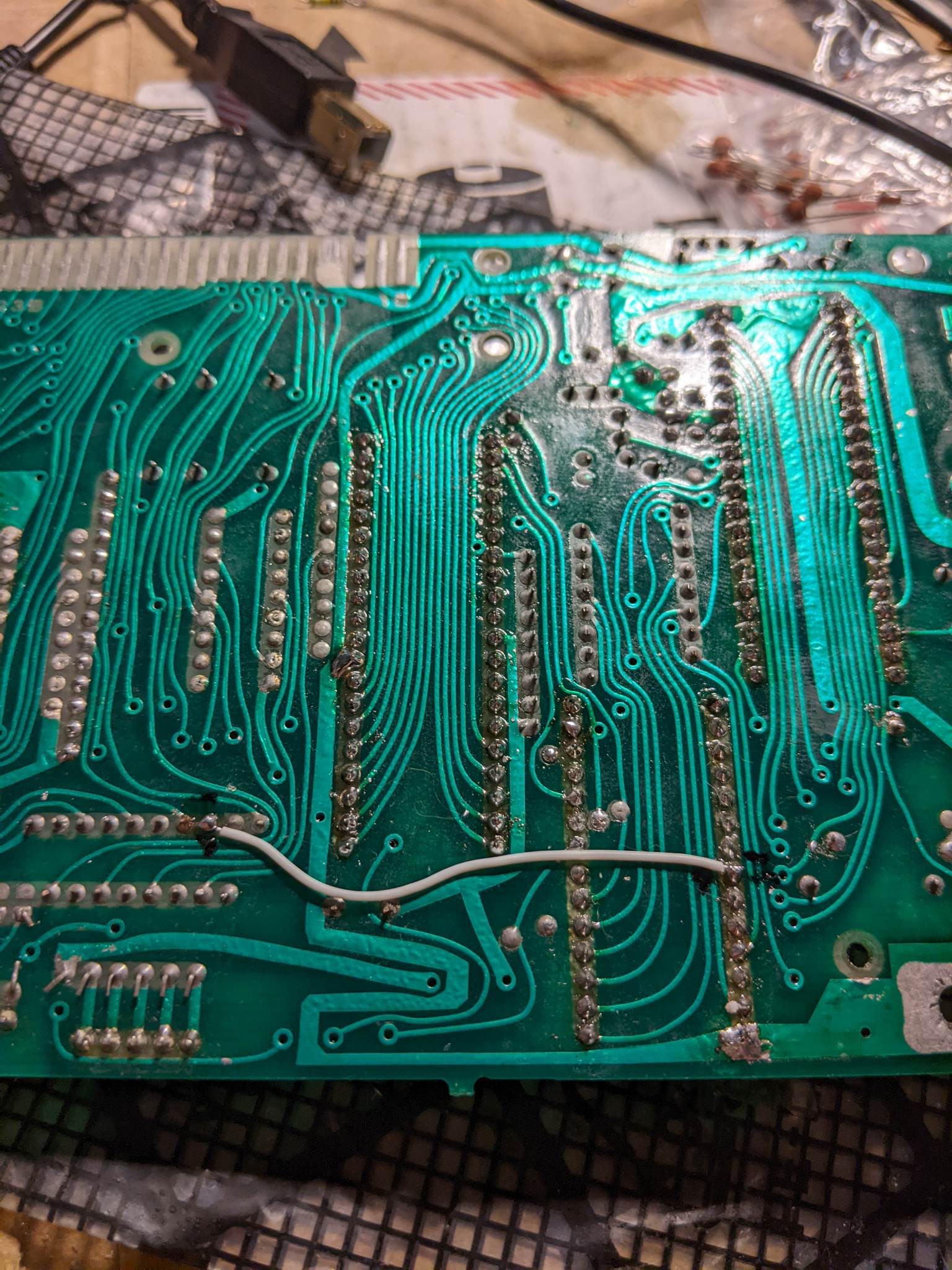 After I replaced the broken trace I plugged everything back in, plugged in the computer and immediately ... got no picture... Its a 40 year old machine with aging corroded parts I have to be realistic and so I half expected this. This lead me down a number of avenues, I wound up toning out all of the traces using the schematics, and replacing the RAM expansion after discovering it was causing some of the lower address lines to stay low.


