-
Masterbuilt Smoker - Front Panel Repair
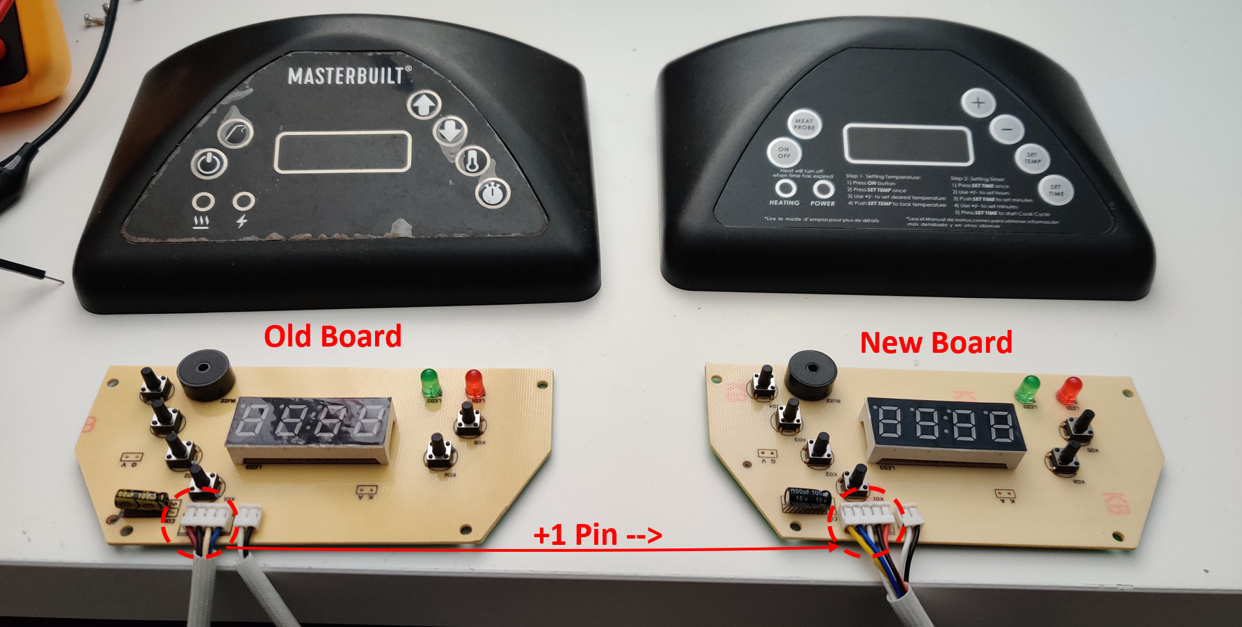
07/25/2024 at 05:46 • 0 commentsA friend of mine has a smoker, who’s front panel circuit recently gave up the ghost. He bought a new one that he thought was compatible but sadly it had an incompatible connector. When I asked him about the symptoms, he said that it couldn’t set the temperature anymore. It was pretty clear on closer inspection that the likely culprit was a mechanical fault on the “set temp” button.
I believe the model of the smoker is “Masterbuilt MB20071117” or something very similar, and the replacement he bought was a “Digital Control Panel Kit Replacement” that seems to be compatible based on the amazon listing… clearly not though, one review even complains “20071117 is a 4 prong connector. This panel has a 2 [and] 5 prong connectors and is not compatible.”
Anyways, here I sit in my lab with a peculiar Masterbuilt smoker panel, and a not so compatible clone.

Busted Buttons
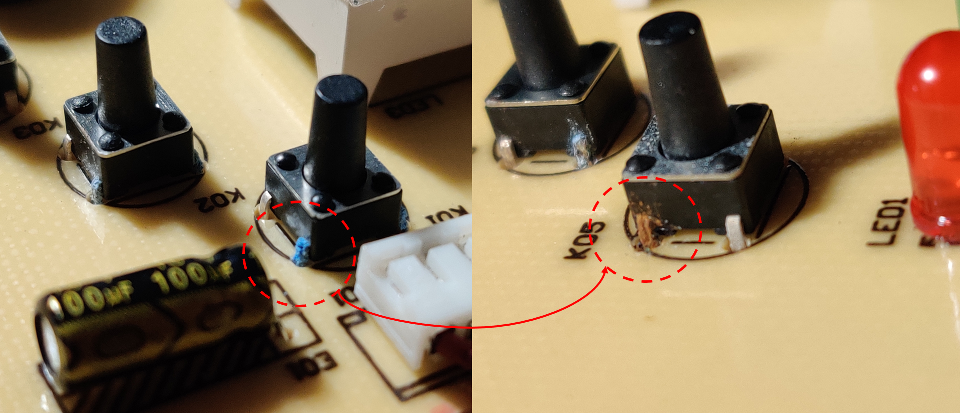
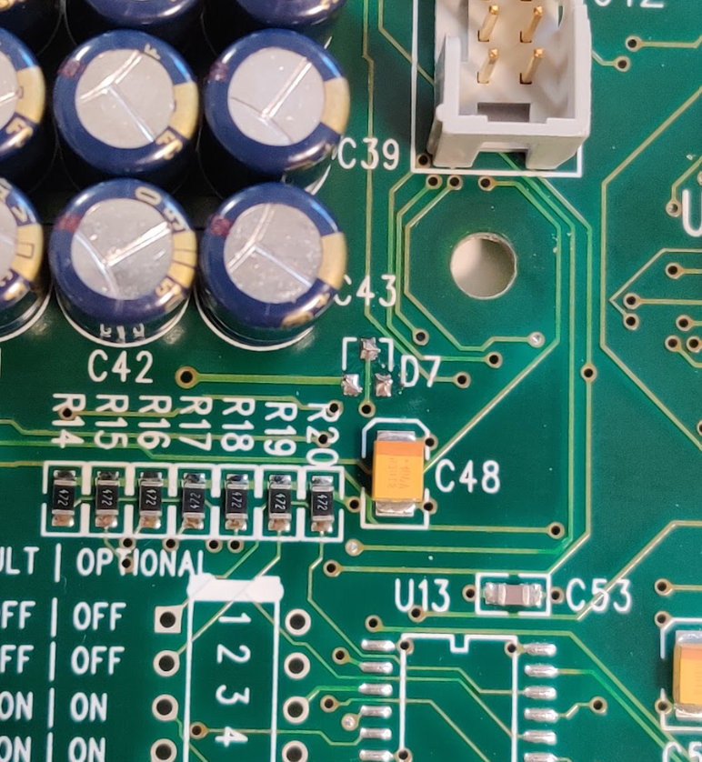
Probing the buttons… I’ve never seen buttons this busted. Scraping away the oxidation I can’t even get a consistent “short” when the button is depressed. All my measurements are in the MΩ range.
Clearly then this is the issue… I have some replacements, but they’re all the shorter style. Alternatively, I could raid parts from the “replacement” new board. Neither of these methods sounds very fun. The boards are covered in conformal coating that can be a pain to solder through.
Alternatively, I could check the circuits and see if I can make the replacement work. This seems more fun so I’ll take this path...
Spider Man Pointing Meme
They’re the same board. It looks like the fab house maybe took some liberties with the copper pours and tooling holes, but other than that (and the extra pin on the connector!) the two circuits are identical.
Gerbers are largely the same, even the silkscreen and ref designators are identical. The only immediate thing that jumps out is C02 doesn’t use a capacitor on the old board… weird. Other than that there’s the following BOM value changes.
Description
NEW
OLD
Should I Care?
R36/35 (LED Limiter)
511 (510 Ω)
201 (200 Ω)
No
R27/26/25… (BTN PU/PD)
222 (2.2 kΩ)
222 (2.2 kΩ)
No
R04/05/06… (7Seg Limiters)
511 (510 Ω)
201 (200 Ω)
No
C02 (Unknown, debounce?)
5101 (5.1 kΩ)1
???nF
Yes
Note 1 – Wasn’t sure if 1015 or 5101. Measure in circuit as 5.09k so I’ll guess the latter.
The good news is the 4th pin isn’t used anywhere. The bad news, they completely changed the wiring so we’ll need to do some pin pulling. Lastly, the confusing news, why is C02 a resistor on our new board?
I’m not too sure what the 2 remaining pins do on the connector. One is power, another is ground and then the remaining 2 go to the IC. One through this CR filter, the other just through a 10k. There’s also that 2wire bundle (black and yellow) that seems to have the same CR filter (now including the 5.1k PD).
My best guess is they’re clock and data lines. Maybe the designer wanted to soften the edges of the signal. (I later realized that one of those signals was for an analog input from a temprature sensor).
Power Up
Lets power the thing up cuz I’m curious. The name on the IC has been removed so I can’t get any help there…. Just by looking at the circuit it seems like the white wire is ground, leaving red as the likely culprit for VCC. I set a low current limit at 3V3, and saw nothing. But the board came to life around 3.7V with a short beep.
When I try to probe the signal connected to C02 (looking for activity maybe), I put the panel into some error mode “EAA1”. Looking into it, it seems to be related to the “smoker's ambient temperature sensor reading too low of a temperature”. The error state latches until you power cycle it.
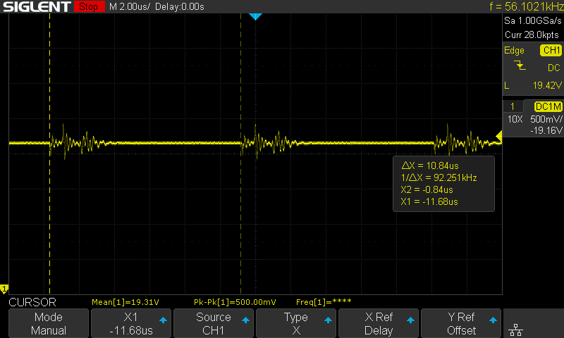
Ok lets treat it like an input then… I wired it up to my function generator and applied 500mV and...
Read more -
Tandy Analog Multimeter Repair
05/25/2024 at 02:25 • 0 commentsHistory
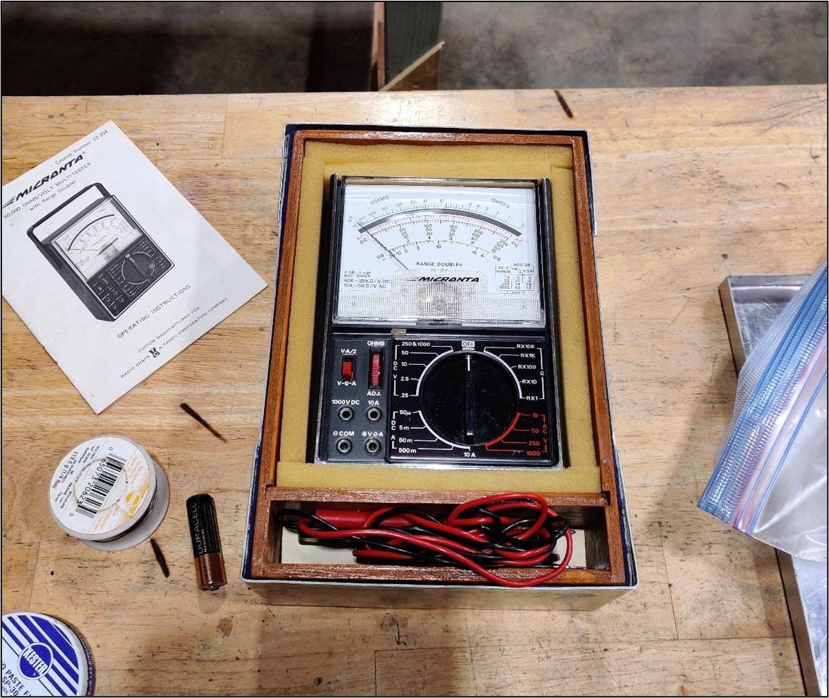
I was pretty excited to be handed my dad’s old multimeter. Tandy!? Radio shack? What are these strange words… I was born in the wrong generation to experience these things first hand, so I was pretty excited to have some genuine Tandy equipment on my bench.
During the multimeter handoff, I was told it might be broken (EVEN BETTER!). We tried turning the device on, and sure enough there was no response… But who can blame the poor thing, its been living in a barn for the past 15+ years.
Schematic
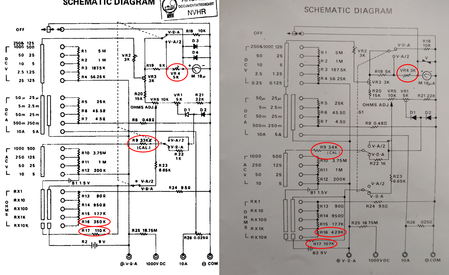
Luckily this multimeter still has its manual with it, but I know not everyone’s that lucky. Here’s the schematic for “Micronta 50,000 OHMS/VOLT MULTITESTER with Range Doubler”, catalog number 22-204.
My schematic looks different from what I found online, specifically R16, R17, R9, VR4. But I suspect, its just a variant of this product. Maybe this schematic will help someone else get out of a rabbit hole. On the right is my schematic, and on the left is theoretically the same schematic found on the web.
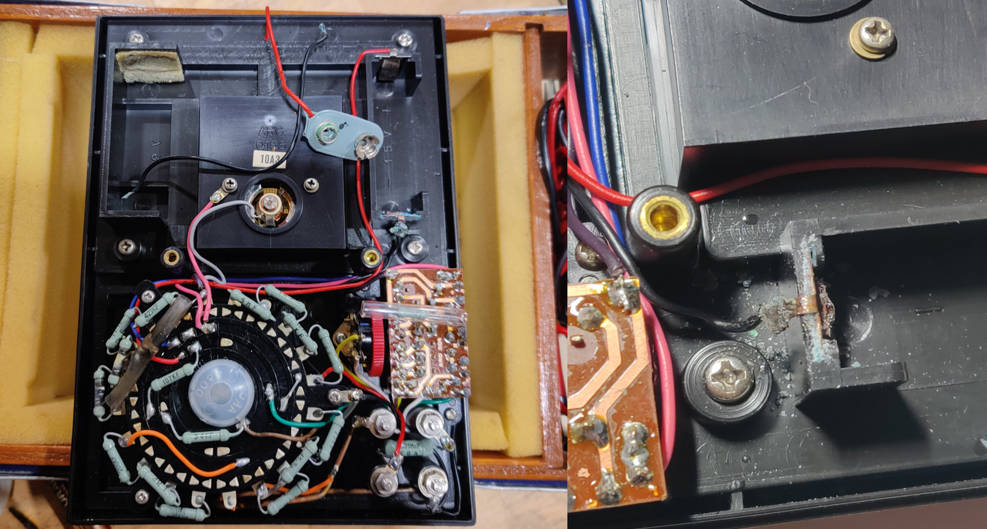
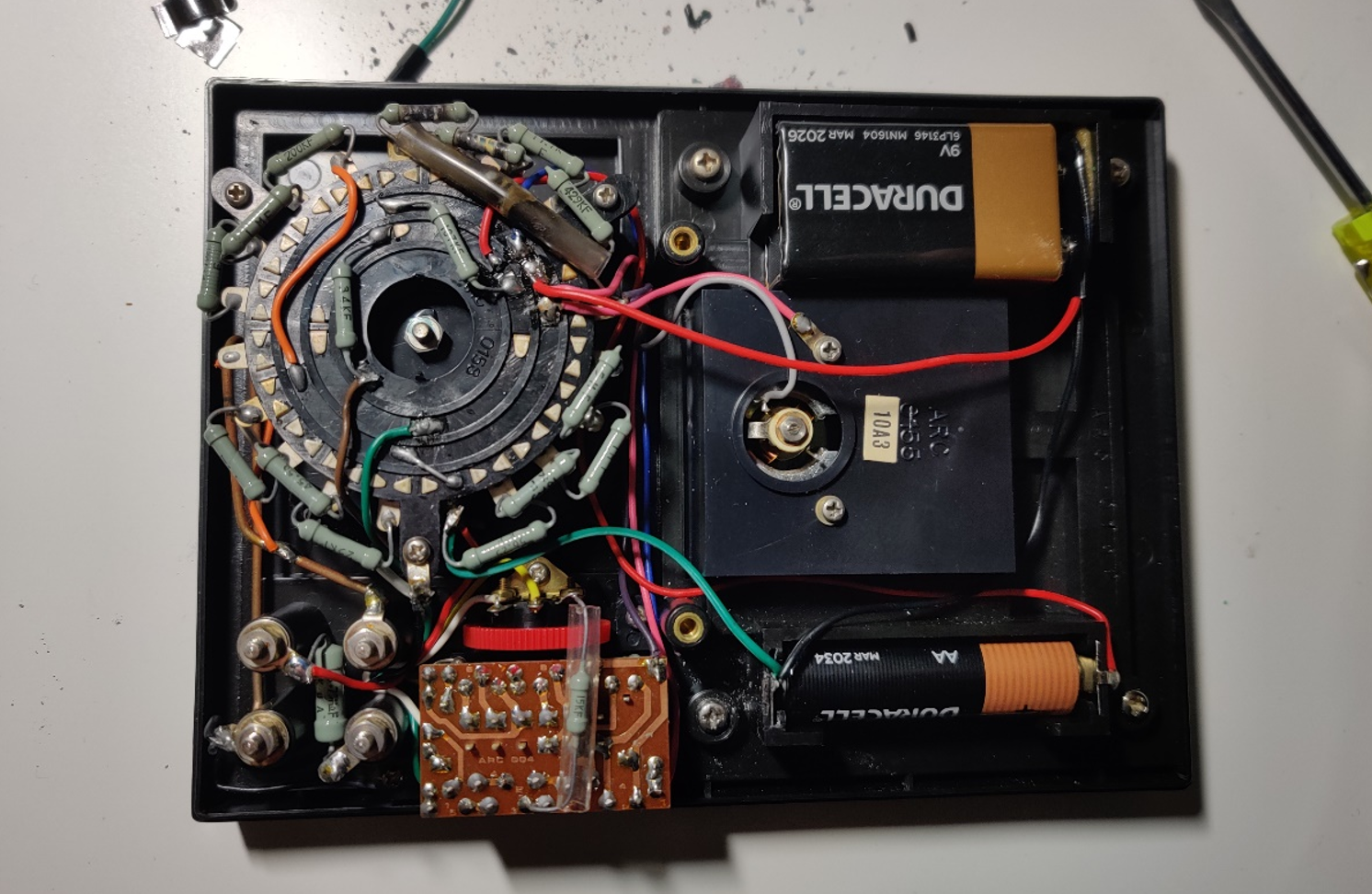
Issue #1 – Battery Terminals
Removing the backplate revealed some nasty corrosion on the mismatched batteries. At first the 9V didn’t look too bad, but when I tried removing it, the cable just “let go” of its solder joint. When I finally pulled the 9V free from its plug, it broke the terminals! I’ll probably try to replace/resolder the 1.5V connector. The aftermath is shown below.
Luckily, I have some extra battery connectors in my parts bin. I replaced both terminals, and plugged in new batteries. Onto the next issue!
Issue #2 – Burnt Resistors
You’ve probably noticed a couple burned parts on the pictures I’ve shown above. It looks like someone tried to measure something with some “umph” while set to measure resistance (specifically 100x). As a result (likely mains voltage) punched its way through R14, R13 and R24.
I had some spare parts to replace these resistors, but it’s a bit of a downgrade. Note, I’m not worried about the performance after my repair… I have two DMM on my bench, this is just a repair for repairs sake. I replaced R14 with ¼ watt 270+680, and R13 with ¼ watt 22+68. For R24 I had to use 3x resistors in parallel (22.1//22.1//67.9). All resistors were verified on a Fluke 87V.
After soldering in the new parts, all is working!
Shown below is a 22ohm resistor being measured. Looks good enough. I also verified the other ranges, as well as the voltage reading. I deem this repaired.
-
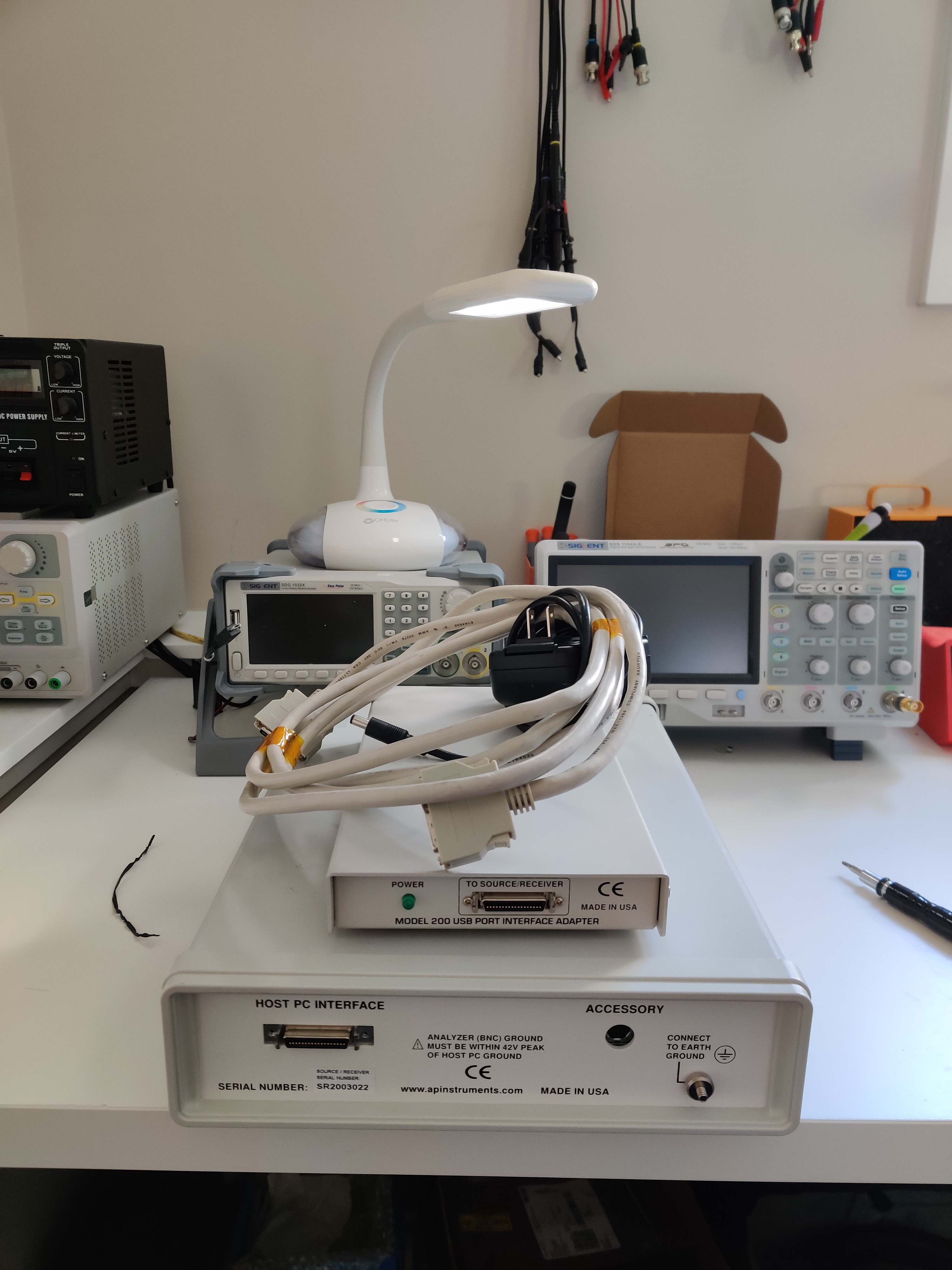
Network Analyzer - Repair
06/15/2023 at 22:34 • 0 commentsI’ve got an AP instruments network analyzer that stopped analyzing. The system is comprised of a USB interface adapter and a main unit. The only symptom is the absence of a power LED on the main unit.
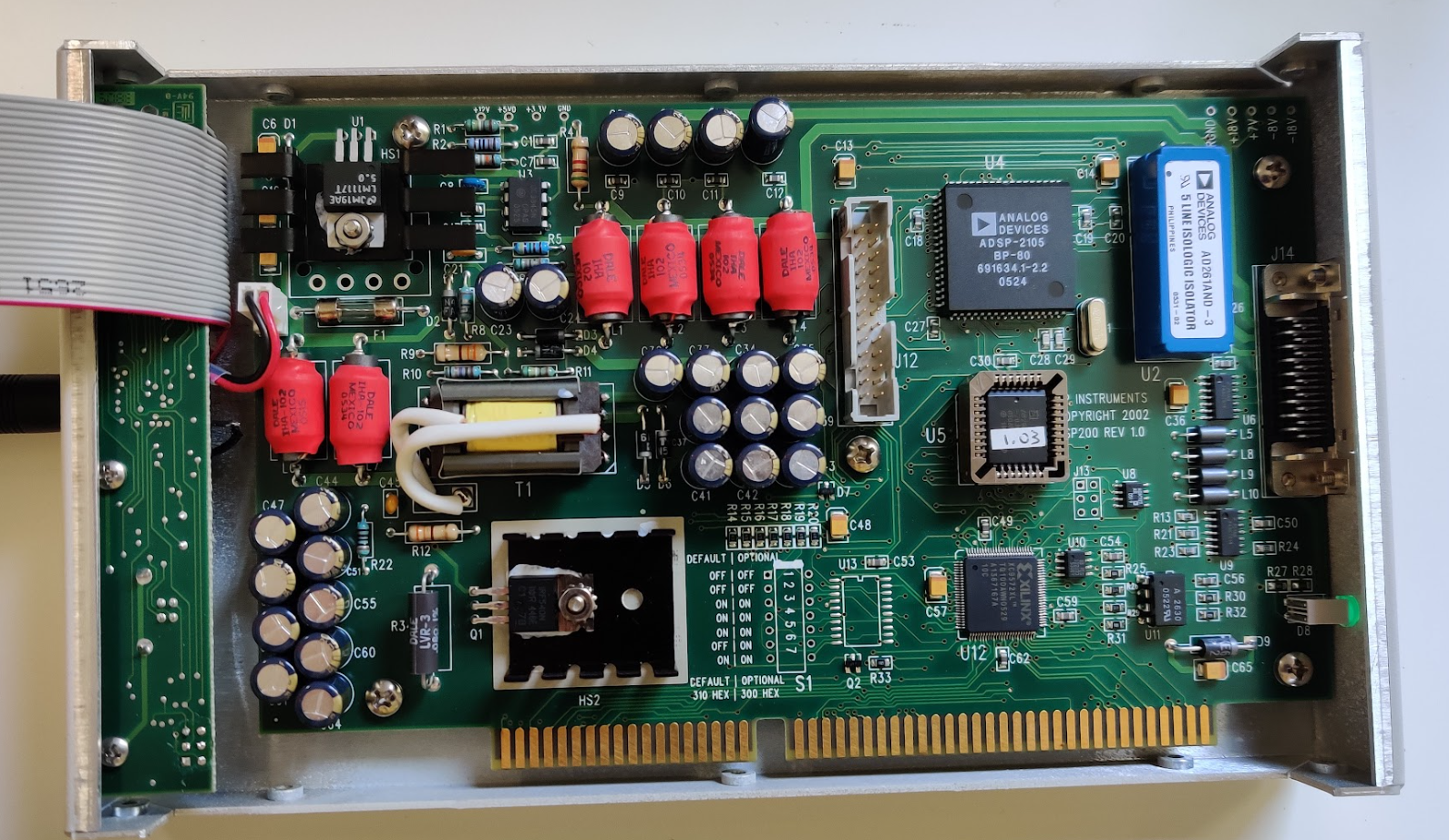
Instead of checking continuity of the cable, (because who am I kidding that’s no fun) I decided to open up the interface adapter.
Luckily, they gave us nice test points we can check right off the bat. All the low voltage rails (12V, 5V, 3V3) look good… but the one’s near the main connector are all zero volts. Maybe it waits for a PG signal before enabling 18V, +7V, -8V.
Next, I did some poking around the board. Seems like one of the main switchers is a UC3845N. VREF and VCC look good, but the switching node "OUTPUT" is held at GND. I’ll dig a bit deeper to see what the other pins are at.
After poking the other pins, it looks like COMP is being used to disable the device. Its being held low (ish) which is stopping the device from starting. Here’s a blurb from the datasheet. This COMP pin is being held low by a XILINX chip…. ☹. That complicates things.
I’m not sure what this chip needs before it will enable the main switcher. Checking the cable, I confirmed that the 12V, 5V, 3V3 rails are NOT sent to the main unit. This means the XILINX chip isn’t waiting for a handshake from anything on that unit (since it won’t be powered).
The suspect chip is a CPLD (XILINX XC9572XL). This isn’t something I can debug.... er atleast not easily.
THE FIX???
My plan is to remove the XILINX's ability to disable the switcher. Luckily there's a diode leading to COMP, so I can simply remove it (D7) and the switcher should work... what's causing the XILINX chip to assert this disable pin though?
And voila, we have voltages. Nothings too accurate, but I was suspicious it wouldn’t be. Shown below is the +18V rail.
Now I’ll try plugging it in, but first I need the software to try and talk to it.
All seems happy. I can’t test the full feature set (I need more BNC cables), but I can at least see that the system is talking ect. I’ll do a final test tomorrow in the lab. (Tested and looks good).
-
Unpowered Digital Isolator Behaviour - ADUM348x
12/10/2022 at 22:45 • 0 commentsOverview:
I was recently working on a schematic that includes some digital isolators (ADUM3480). For power sequencing reasons, I need to operate the chip with the input side powered while the output is unpowered. My concern is… will the signals couple through from the input (powered side) to the output (unpowered) side?
The datasheet (here) doesn’t clearly define this quasi-unpowered behaviour, so I thought it best to do some testing. And, while I’m at it, I may as well document my findings.
TLDR:
If the output is unpowered, then no notable activity will be observed at the output, regardless of what signals are being sent at the input side.
The general test setup / procedure is as follows:
- Configure device on breadboard… 100nF decoupling for all PWR pins. V_{DDL1}, V_{DDL2}, V_{DD1}, V_{DD2}, V_{DDC1}, and V_{DDC2}.
- Tie all unused inputs to GND_{1} via a 10kohm resistor
- Power input V_{DDL1} and V_{DD1} at 3.3V to 5V, and power output V_{DDL1} and V_{DD1} at 3.3V to 5V
- Apply square wave to one input channel V_{Ix}
- Observe all pins on output (isolated side)
- Disconnect the output power from V_{DDL2} and V_{DD2} and repeat step 4/5
Test gear used:
- Isolated PSU – BK Precision Model 1670 DC Power Supply (3 isolated channels)
- Function Gen – SDG 1032X
- Oscilloscope – SDS 1104X
Results:
The initial sanity check confirmed the chip was functioning normally (step 3 to 5). The 3V3 input signal, and 5V output are shown below. Note these two signals couldn’t be captured in the same image since I don’t have isolating probes… and I didn’t want to short the two isolated GND’s.
Figure 1 - Input signal
Figure 2 - Output Signal
Next, I disconnected the 5V supply at the output, while leaving the input 10kHz square wave on V_{IB}. The output channel V_{OB} is shown below. We can see minor activity at the output (periodic spikes), likely caused by capacitive coupling.. since these spikes correspond to the edges of the input signal.
Figure 3 - Input Powered, Output Unpowered, Output signal
Next, I repeated the test with an input voltage of 5V, hoping to provide a worst case for capacitive coupling. There was a negligible change from the 3V3 test.
Caveats of these results:
Reminder that this test was conducted without any forced potential difference across the isolation barrier. I'm not sure how a 1kV difference between GND_1 and GND_2 might affect these results. I would think the results would be much the same, but I'm not very well versed in high voltage design.