Integrated Circuits (ICs) have revolutionized the electronics industry by enabling the miniaturization of electronic devices and systems. From smartphones to medical devices, ICs are foundational to modern technology. This article will introduce what ICs are, explore several major types, and provide a summary along with answers to some common FAQs.
What is an Integrated Circuit?
An Integrated Circuit (IC) is a semiconductor device that consolidates multiple electronic components, such as transistors, resistors, and capacitors, into a single chip. These components are interconnected to perform specific functions within electronic systems. The development of ICs allowed for the miniaturization and increased efficiency of electronic devices, making them integral to modern technology.
Major Types of Integrated Circuits
1. Analog Integrated Circuits
Analog ICs process continuous signals, such as sound and light, rather than digital signals. They are used in a variety of applications including:
Operational Amplifiers (Op-Amps): Used in signal amplification and filtering.
Voltage Regulators: Maintain a consistent voltage level.
Analog-to-Digital Converters (ADCs): Convert analog signals into digital data.
2. Digital Integrated Circuits
Digital ICs handle binary data (0s and 1s) and are fundamental to computing and digital communication. Key examples include:
Microprocessors: The central processing units (CPUs) of computers, executing instructions and performing calculations.
Memory ICs: Include RAM (Random Access Memory) and ROM (Read-Only Memory) used for data storage.
Logic Gates: Basic building blocks for digital circuits, performing logical operations like AND, OR, and NOT.
3. Mixed-Signal Integrated Circuits
Mixed-signal ICs combine both analog and digital functions on a single chip. They are essential in applications where analog signals must be processed alongside digital data. Examples include:
Analog-to-Digital Converters (ADCs): Convert analog signals to digital form for processing by digital systems.
Digital-to-Analog Converters (DACs): Convert digital data into analog signals.
4. Radio-Frequency Integrated Circuits (RFICs)
RFICs are designed to handle high-frequency signals and are crucial for wireless communication. They are used in:
Cellular Phones: For transmitting and receiving radio signals.
Wireless Communication Devices: Such as Bluetooth and Wi-Fi modules.
5. Power Management ICs
Power Management ICs regulate and distribute power within electronic devices. They include:
Voltage Regulators: Ensure stable voltage supply.
Battery Management Systems: Optimize battery performance and longevity.
Summary
Integrated Circuits are pivotal in the electronics industry, providing the backbone for a wide range of applications from computing to communications. Understanding the different types of ICs—analog, digital, mixed-signal, RFICs, and power management—can help in selecting the right component for specific needs and applications.
1. What is the difference between analog and digital ICs?
Analog ICs handle continuous signals and are used in tasks like signal amplification, while digital ICs process binary data and are used in computing and data storage.
2. Why are Mixed-Signal ICs important?
Mixed-Signal ICs integrate both analog and digital functions, allowing for efficient processing of signals that involve both types of data, such as in audio and communication devices.
3. What are some common applications of RFICs?
RFICs are commonly used in wireless communication devices, including mobile phones, Bluetooth devices, and Wi-Fi modules, where high-frequency signal processing is required.
4. How do Power Management ICs improve device performance?
Power Management ICs ensure that electronic devices receive a stable and appropriate power supply, optimize battery usage, and enhance overall device efficiency...
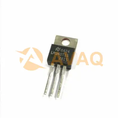
The IC 7815 is a widely used voltage regulator in electronic circuits, designed to maintain a stable +15V output despite variations in the input voltage. As part of the 78xx series of voltage regulators, it plays a crucial role in ensuring that electronic components receive a consistent and reliable power supply. This article delves into the features, applications, and usage of the IC 7815, providing a comprehensive overview of this essential component.
Key Features of the IC 7815
The IC 7815 is characterized by its ability to provide a fixed output voltage of +15V, making it ideal for circuits that require a stable power supply. Here are some of its key specifications:
Output Voltage: The IC 7815 delivers a constant +15V output, which is crucial for powering sensitive electronic components.
Input Voltage Range: To function correctly, the input voltage should be at least 17V and can go up to 35V.
Output Current: This regulator can supply up to 1.5 amperes (1.5A) of current, making it suitable for various applications.
Thermal and Short-Circuit Protection: The IC 7815 includes built-in protection features such as thermal overload and short-circuit current limiting, enhancing its reliability in different environments.
Package Availability: It is available in multiple packages like TO-220, TO-3, and D2PAK, providing flexibility in its usage across different designs.
Applications of the IC 7815
The IC 7815 is a versatile component with a wide range of applications. Here are some common uses:
Powering Microcontrollers and Sensors: The IC 7815 is frequently used in circuits that power microcontrollers and sensors, ensuring they receive a steady +15V supply.
Current Limiting: It can act as a current limiter in applications where it is necessary to control or restrict the flow of current to prevent damage to other components.
Voltage Stabilization in Audio Amplifiers: In audio circuits, the IC 7815 helps stabilize the voltage, leading to consistent and distortion-free audio output.
Battery Charging Circuits: The regulator is often employed in battery charging circuits, maintaining a stable voltage output during the charging process.
Industrial Automation Systems: In industrial settings, the IC 7815 is used to regulate the voltage supplied to control modules and sensors, ensuring their proper operation.
IC 7815 Equivalent Parts
In cases where the IC 7815 is unavailable or if an alternative is preferred, several equivalent parts can be used:
LM340-15: A positive voltage regulator with similar output voltage and current specifications.
LM7915: A negative voltage regulator offering -15V output, suitable for circuits requiring complementary voltage regulation.
LM317: An adjustable voltage regulator that can be set to provide a +15V output with appropriate external components.
Practical Application: Power Supply Circuit with IC 7815
A practical use case of the IC 7815 involves its integration into a power supply circuit. This setup typically includes a MOSFET to regulate voltage, with the IC 7815 controlling the output to ensure a consistent +15V supply. Additional resistors and capacitors are used to stabilize the circuit and eliminate oscillations, especially at higher frequencies. This configuration is common in laboratory power supplies and industrial automation systems where precision and reliability are paramount.
Conclusion
The IC 7815 is a fundamental component in many electronic circuits, offering a reliable and stable +15V output. Its versatility and built-in protection features make it an essential choice for powering microcontrollers, sensors, and other sensitive components. By understanding its pin configuration, the role of capacitors, and potential equivalents, you can effectively incorporate the IC 7815 into a wide range of applications, ensuring your circuits operate smoothly and efficiently. Whether you’re working on an industrial automation system or a simple audio amplifier, the IC 7815 remains a go-to solution for fixed voltage...
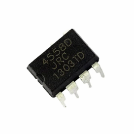
The JRC4558 is a dual operational amplifier integrated circuit (IC) manufactured by Japan Radio Corporation (JRC), now part of New Japan Radio (NJR). It's a versatile component used in various electronic applications, particularly popular in guitar pedals and audio circuits.
Known for its robust performance, it offers strong input impedance, substantial voltage amplification (with a gain of up to 100dB), and operates within a wide power supply range (from ±4V to 18V). This IC contains two separate op-amps within its 8-pin package and is available in different formats such as DIP (Dual Inline Package) and SOP (Small Outline Package). Its flexibility and reliability have made it a favorite among engineers, hobbyists, and musicians for decades.
What is TL072
The TL072 is a popular dual low-noise JFET-input operational amplifier (op-amp) manufactured by Texas Instruments. It's part of the TL07x series known for its high input impedance, low noise, and wide bandwidth.
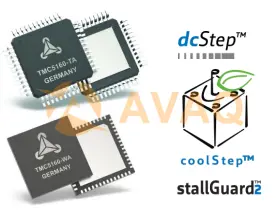
The TMC5160/TMC5160A is a high-power stepper motor controller and driver IC with serial communication interfaces. It offers a flexible ramp generator for precise target positioning and features the industry's most advanced stepper motor driver. By using external transistors, it enables the creation of highly dynamic, high-torque motor systems.
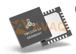
What is TMC2209
The TMC2209 is an ultra-quiet motor driver IC designed for two-phase stepper motors. Its pinout is compatible with several legacy drivers and the TMC2208. Featuring TRINAMIC's advanced StealthChop2 technology, it ensures noiseless motor operation, maximum efficiency, and optimal torque. With fast current regulation and the option to use SpreadCycle, it allows for highly dynamic motion and includes features like StallGuard for sensorless homing.
Main Differences between TMC5160 vs TMC2209
From Features and Application, let's see the differences between TMC5160 vs TMC2209
Features
Feature
TMC5160
TMC2209
Suitable for
2-phase stepper motors (1 to several 10A)
2-phase stepper motors (up to 2.8A peak)
Voltage Range
8V to 60V DC
4.75V to 29V DC
Communication Interfaces
SPI & Single Wire UART
Single Wire UART & OTP
Microstepping Support
Up to 256 microsteps per full step
Up to 256 microsteps by MicroPlyer™
Special Control Features
SixPoint™ ramp, Resonance Dampening, DcStep™
StallGuard4™, CoolStep™
Noise Operation
StealthChop2™
StealthChop2™
Current Control
CoolStep™ for energy savings
CoolStep™ for energy savings
Protection & Diagnostics
Full Protection & Diagnostics
Full Protection & Diagnostics
Package Size
Compact 7x7mm² TQFP48 package
Compact QFN package with large heat slug
Applications
TMC5160 Application
High-Power Stepper Motors: The TMC5160 is suitable for applications that require driving high-power stepper motors with coil currents ranging from 1 to several 10A. This makes it a good choice for applications where higher torque and power are needed, such as industrial automation and CNC machines.
Precise Positioning: It offers features like SixPoint™ ramp, high microstepping resolution (up to 256 microsteps per full step), and encoder interface, making it suitable for applications where precise and smooth positioning is critical.
Quiet Operation: With features like StealthChop2™ and resonance damping, the TMC5160 provides noiseless operation, making it ideal for applications where low noise is essential, such as 3D printers and medical devices.
Advanced Control: Its advanced control algorithms and communication interfaces (SPI and Single Wire UART) make it a good fit for applications that require fine-tuned control and diagnostics.
TMC2209 Application
Low to Medium Power Stepper Motors: The TMC2209 is designed for driving 2-phase stepper motors with coil currents of up to 2.8A (peak) or 2A RMS. It is suitable for applications with lower power requirements, such as 3D printers, smaller CNC machines, and robotics.
Cost-Effective Solutions: TMC2209 offers a balance between performance and cost, making it a preferred choice for applications where cost-effectiveness is a priority.
Silent Operation: Like the TMC5160, it incorporates StealthChop2™ technology, providing silent motor operation. This is beneficial in applications where noise reduction is desired, especially in consumer electronics and small-scale automation.
Ease of Use: TMC2209's straightforward STEP/DIR interface and support for MicroPlyer™ interpolation simplify the integration process, making it a good choice for hobbyist and entry-level applications.
Energy Efficiency: It features CoolStep™ current control, which can save up to 75% energy. This is advantageous in applications where energy efficiency is a concern.
The LT9611UXC is a multimedia converter chip manufactured by Lontium Semiconductor Corporation. It is designed to convert MIPI DSI (Display Serial Interface) and CSI (Camera Serial Interface) signals to HDMI 2.0 output. This makes it a valuable component for connecting MIPI-based displays or cameras to HDMI displays or monitors, especially in applications requiring high-resolution video and data transfer.
LT9611UXC Specifications
Single/Dual-Port MIPI DSI/CSI Receiver:
Compliant with D-PHY 1.2, DSI 1.3, and CSI-2 1.3 standards.
Integrated DSC 1.2 decoder.
Configurable as 1 or 2 ports.
Supports 1 clock lane and 1, 2, 3, or 4 configurable data lanes per port.
Data lane speeds ranging from 80 Mbps to 2 Gbps per lane.
Skew calibration for optimal signal integrity.
Programmable receiver equalizer.
Supports data lane swap (arbitrarily) and polarity inversion (independent).
3D support: can receive L and R frames or alternate odd-L/even-R pixels.
Supports DSI in both burst and non-burst modes.
DSI supports various video formats with or without DSC/CSC.
Digital Audio Input:
I2S interface supporting 2-channel audio with various sample rates (32-192 kHz) and sample sizes (16-24 bits).
SPDIF interface supporting PCM, Dolby Digital, and DTS digital audio at up to 192 kHz frame rate.
IEC60958 or IEC61937 compatible.
HDMI 2.0 Transmitter:
Compliant with HDMI 2.0b, HDMI 1.4, and DVI 1.0 standards.
Compliant with HDCP 2.2 and HDCP 1.4.
Supports a high data rate of up to 6 Gbps.
On-die back termination.
Programmable transmitter swing and pre-emphasis.
AC-couple capable.
Supports channel swap (arbitrarily) and polarity inversion (independent).
Capable of supporting 4K resolution at 60Hz.
Supports 3D formats (side-by-side/full).
Supports various video formats with or without DSC/CSC.
HDR (High Dynamic Range) support.
TMDS scrambling for EMI/RFI reduction.
Supports SCDC (Status and Control Data Channel).
5V tolerance for DDC (Display Data Channel) and HPD (Hot Plug Detect) I/Os.
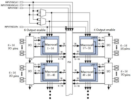
A Complex Programmable Logic Device (CPLD) is a type of digital logic device used in digital circuit design and implementation. CPLDs are part of the larger family of programmable logic devices (PLDs), which also includes Field-Programmable Gate Arrays (FPGAs).
Here are some key characteristics and features of CPLDs:
Programmability: CPLDs are programmable digital logic devices, which means their internal logic functions can be configured or programmed to perform specific tasks or functions. This programming typically involves specifying the logical connections and behavior of the device.
Logic Blocks: CPLDs consist of a collection of programmable logic blocks that can be configured to perform various logical functions (AND, OR, XOR, etc.). These logic blocks are interconnected to form the desired digital circuit.
Interconnectivity: CPLDs have a programmable interconnect structure that allows designers to create custom routing for signals between the logic blocks. This flexibility in routing helps in implementing complex logic functions efficiently.
Inputs and Outputs: CPLDs have a certain number of input pins (for receiving external signals) and output pins (for driving external signals). The number of inputs and outputs varies depending on the specific CPLD model.
Macrocells: CPLDs often include macrocells, which are configurable elements that can implement various functions, such as flip-flops, latches, and combinational logic. Macrocells are used to store intermediate results and synchronize signals.
In-System Programming: CPLDs can be reprogrammed in-system, which means they can be updated or modified without removing them from the circuit board. This feature is useful for design iteration and debugging.
Lower Complexity: CPLDs are generally smaller and have less capacity compared to FPGAs. They are well-suited for simpler logic designs and applications where lower power consumption is desired.
Deterministic Timing: CPLDs offer deterministic timing characteristics, which means that the propagation delay of signals through the device is predictable and consistent. This feature is essential in applications where timing is critical.
Applications: CPLDs are often used in a variety of applications, including control systems, glue logic, interface logic, and small-scale digital signal processing (DSP). They are particularly useful for tasks where a custom logic function is needed, but a full-scale FPGA might be overkill in terms of size and power consumption.
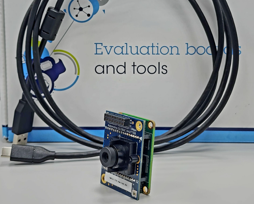
The VB56G4A is a 1.5 MP pixel global shutter image sensor designed for automotive driver monitoring applications. Using the superior 3D stacking technology and ST patented process, the sensor performs excellent in the near infrared region (940 nm). Thanks to backside illumination technology (BSI) and its excellent sensitivity, the VB56G4A can be operated with a simple LED or VCSEL. This makes them ideal for applications such as driver monitoring systems (DMS).
And in order to help customers evaluate and verify the image quality, ST launched a miniaturized development board (CX3)_ as shown below:
►Core technical advantages
1.) High sensitivity: improved quantum efficiency (Quantum efficiency), greatly improving the performance in invisible light (Near IR). And has a high modulation transfer function (High MTF) 2.) Small footprint (Small footprint): Stack BSI 3.) Embedded ISP : -5x5 dynamic defect pixel correction _Auto Exposure Control 4.) Machine vision application support _24x14 area statistics _4 frame contexts, quick switches and sequences _LED strobe control output, flexible timing
1.5-megapixel image sensor in a small package • Global shutter architecture, 3D stack sensor 40 nm/65 nm • 2.61 µm x 2.61 µm BSI (backside illuminated) pixels • 1.5-megapixel monochrome sensor (1124 x 1364)
Package: OBGA • Dimensions: 6.2mm x 6.9mm
Easy to integrate • Built-in automatic exposure function • Programmable sequence : 4-frame contexts • 8 programmable GPIOs _NIR (near infrared) illumination control output, synchronized with sensor integration period _PWM (pulse width modulation) control _Master/Slave external framework starts • Automatic dark calibration • Dynamic Pixel Defect Correction • Image cropping • Mirror/flip readout • Binning and subsampling (x2 and x4) • Typical power consumption: 145 mW at 60 fps • Dual lane transmitter MIPI CSI-2 up to 1.5 Gbps per lane
Unique image performance • Peak quantum efficiency 24% @ 940 nm • Linear dynamic range up to more than 60 dB • Up to 88 frames per second at full resolution