-
Tearsday Thurdown #5
08/19/2023 at 04:03 • 0 commentsThe Involuntary Teardown of the WF-1000XM4 Charging Case
I was cycling back home from a Saturday brunch blasting the funky audio waves of Franc Moody through my best earphones to date, the Sony WF-1000XM4 earbuds. I got home and performed the ritualistic wallet, keys, phone, earbud case pocket haka. There was no earbud case present in my pocket. I retraced my steps and sure enough they had fallen out of my pocket in the middle of an intersection whilst cycling. Sure enough the form factor was now very slimline and design somewhat minimalistic with all parts having been cold rolled several times by the local neighbourhood SUVs. Here’s a great indepth teardown: https://www.qucox.com/sony-wf-1000xm4-teardown/. The housing was completely jodido (munted/smashed/fucked in Spanish), so this will be brief.
The Housing
The outside of the case was a premium matte black plastic with a glossed plastic on the inside. The assembly of the all the components during use was very snug, with that solid dense feeling even though much of the plastic wall used was very thin <1mm. A piece of foam was embedded in the plastic to ensure the battery was safe from any impacts or the ever dreaded Lipo swelling. There were three magnets recovered (out an assumed total of four). These were extremely strong and had gathered many of the SMD components during the cold rolling process of the charging case. Likely neodymium, n52 grade.
The Circuitry
The circuitry was also jodido, so the only things of note we can see are the custom induction charging coil, the charging USB C port and the small 520mAh single cell Li-ion. Also there was a flexible ferromagnetic material inbetween the battery and the copper coil, to redirect/sink the magnetic field coming from the wireless charging emitter. Here’s an interesting article about electromagnetic lensing of radiowaves using a ferrite core: https://en.wikipedia.org/wiki/Ferrite_core#Ferrite-rod-aerial
As for the earbuds, these are by far the best noise cancelling earbuds I have ever tried with a sound quality that’s hard to match with any other earbud.
-
Tearsday Thurdown #4
05/12/2022 at 08:41 • 0 commentsTearing into Sony WH-CH510 headphones
These headphones were stolen off a friend who had owned them for many years as he was going to throw them out. Why were they bin worthy? A piece of plastic snapped on one headphone, which I was able to fix with a bit of super glue. These are still in great working condition even with the thoroughly worn ear cushions.
Housing
The mechanical design of the headphones are simple the plastic curved piece of plastic has a good amount of spring to hold the headphones over a large head and could be adjusted with a sliding mechanism with multiple soft locking notches. The headphones are very lightweight so let’s open them up to see what’s inside.
The first step is to remove the ear cushions from the headphones, which exposes three screw holes.Once the screws in these three holes have been removed you can proceed to separate this plastic plate, by levering a small flathead screwdriver into the bottom, where there is a notch in the plastic plate. Now we can see inside the headphones!
To the electron city! (aka PCB)
All of the circuitry for this device is located in the right headphone housing as seen below. This circuit is very simple and has similar components to my first teardown of some wireless earbuds. However these headphones have a much larger volume of space, sizing constraints are much less of an issue (boring!). The major components we can see when we open the housing is a 3.7 V Lipo battery, a small conical speaker and the main PCB.
On the circumference of the PCB from left to right we have three tactile switches and LED connected to a lightpipe and a USB C charging port. The top of the PCB has very few components; only passive components like resistors, capacitors, and test points are present on this side. We call also see ‘through via’ stitching throughout the board to shield the RF parts of the circuit and ensure impedances of radio frequency lines are controlled. To reveal the other side of the PCB we simply unscrew one black screw near the centre of the PCB.
The rear of the PCB is also very simple. We have the power management circuit next to the USB header, the micro in the centre of the board and what looks like some FETs, diodes and maybe a regulator sparsely scattered around the rest of the board. The crab logo is a clear indicator that this is a Realtek SoC (RTL8763BFS). This SoC contains a silly amount of features including:
- Low power DSP - dedicated filtering microphone data and a 24bit audio codec
- Integrated dual switch mode power regulator, linear regulators, and battery charger; charging current up to 400mA
- Bluetooth radio - BLE, BT 5.0 and BDR/EDR
- USB 2.0 and USB C compatibility
- 32-bit ARM Cortex-M4F Processor
Amongst many other features somehow packed into one small package.
Below the SoC we can see a 40MHz crystal oscillator. Surrounding the SoC in close proximity are of course the decoupling/bulk capacitors.
To the left of the PCB we have an PCB trace antenna which will have all of its trace and components specifically sized to a specific impedance to optimise the radiation power of the antenna. There seems to be a blue multilayer chip antenna of sorts attached to the end of the PCB trace antenna. It is difficult to know how this antenna setup works without learning more about the intricacies of antenna engineering and the relevant electromagnetic physics principles. This is meant to be a good site for mere laymen who want to learn about antennae from fundamentals -> https://www.antenna-theory.com/ .
Conclusion
Overall a very simple teardown with proof that complex circuitry isn’t required at all when you can find a SoC that can do it all from power management to radio to processing etc. A fun quick easy teardown. They worked perfectly when put back together ready to push more well timed air pressure waves into my ears!
-
Tearsday Thurdown #3
04/21/2022 at 09:40 • 0 commentsGarmin Vivoactive 1 teardown
I’ve had this Garmin Vivoactive for over 6 years now and upgraded a couple of years ago to the Garmin Forerunner 45 for running and swimming. The old Vivoactive used to have the stamina of a rabbit in bed (it had a great battery life), but the battery life rapidly deteriorated as I was starting to use it a lot less. The watch strap completely broke on one side so I replaced it with a piece of janky elastic. It still functions well, taking a reasonable amount of time to pick up some solid GPS satellite signals. Enough chit chat let’s tear in!
How do we open a waterproof watch??
The housing of the Vivoactive is very sleek and much thinner than many other current smart watches(8mm vs 12mm for my Forerunner 45), but also has much less features. After a good few minutes of inspecting the watch for any edges to pry open I noticed a change of material between the watch face and housing. I assumed like in other devices (such as phones and the Kaiser Baas teardown that the screen was simply glued on. Being a water-tight device my smallest tools could not pry the screen off, so I use an iron to soften the glue holding the screen down. I then used a small suction cup to pull on the screen, which lifted a small edge to be pryed open as seen in the figure below. This has definitely ruined the original 5 ATM waterproof rating of the watch.
The insides
After very carefully prying off the LCD/touchscreen the quite simple insides were exposed. The main visible components were the
- Lipo battery, 150mAh, 3.7v
- PCB
- Antenna
- Flex PCB interconnect
The antenna is made by TE and sits on three pins protruding from the PCB. A small connector sits under the antenna, which could be used for programming or other testing purposes. The push buttons on either side of the PCB are supported with a resin substance. The main IC seen on the right side of the PCB is a Nordic nRF51422 BLE, ANT and 2.4 GHz SoC. A great SoC for a wearable device, with plenty of computing power with its M0 core, flexible radio usage, and low energy modes. There is an external 32MHz crystal oscillator adjacent to and driving the Nordic chip.
In the centre of the PCB we can see a low profile FPC connector. All of the the components look to be 0201 as expected with a wearable device of this size. There is a farm of caps and resistors on the left side of the PCB likely a mixture of decoupling caps and peripheral components for setting up IC parameters.
The dark side of the PCB
To access the other side of the PCB the LiPo battery is gently levered out and the four conductive ‘power’ screws are removed. Upon removal and flipping over the PCB we find that the other side is completely boxed in and shielded. Half of the metal shield is covered in copper tape with the other half of the laying under the battery. Under this side we likely have an IMU, a GPS module and adjoining circuitry.
The antenna is provided by TE connectivity and has a PN that looks like 2??8462. To aid the rf part of the PCB we have a keepout copper area between the antenna and the SoC. There is a component between the antenna and the SoC which is likely to be some kind of impedance matching/ signal conditioning circuit. We can also see ground plane stitching around the perimeter of the PCB, in particular near the antenna. There are many exposed circular gold plated test points
on the PCB, likely for use with an ICT method like flying probe or bed-of-nails.
The screen used for the watch uses memory in pixel (MIP) technology where the LCD pixels required a very low power to stay ON. This is evident as the screen does not emit light but uses ambient light to illuminate the screen or a backlight on demand. The screen is also a touch screen for extra UI functionality.
The charging case
The charging case was simple to pull apart, only held together with glue. There is a single component PCB in the case with a 2A fused attached to the positive...
Read more -
Tearsday Thurdown #2
03/04/2022 at 08:19 • 0 commentsTearing down a Kaiser Bass X200 Action Camera
Today we're taking apart a Kaiser Bass X200 Action camera I took on a hiatus to Europe and Central Asia for a few months. This camera has been through the wars it's been used in in Kazahk sand, Turkish water and Mongolian dirt. It was great for taking photos, however it's video quality was terrible. Video quality was similar to 240p with a non-constant frame rate.
Housing
The first step as usual is to tear into the housing. Firstly the lithium ion battery (3.7v 900mAh, 3.33Wh) was removed to find the opening point of the housing. This exposed an easy place to pry the face-plate from the main body of the housing.
With the face plate removed, this exposes four corner screws, a power button PCB, and a small coin shaped speaker down the side of the camera. The screws are removed to reveal the LCD screen and motherboard.
The LCD screen is slotted into the housing. There is a highly diffuse sheet light guide (backlight) behind the LCD screen illuminated by three right angle LEDs beside the ribbon cable.
The Motherboard
Power
The top of the PCB is likely the power supply part of the board where we can see an inductor and an 8SOIC boost converter, which steps up/down the battery voltage for the various circuits on the rest of the board. The chip with the CNVL marking in the top left corner is a low voltage detector. This chip will actively output a high or low signal whenever the input voltage drops below 3v, to protect the device from brown out related failure. I assume many of the capacitors in the top part of the PCB are decoupling caps for the main MCUs power supply input.
The Smarts
The ribbon connector in the centre of the board is for the LCD screen. The PUYA 8 pin IC on the mid-left side of the board is flash memory for the MCU likely required for storage of images before they are transferred to the SD card and just extra memory for the program running on the MCU. The SD card slot is obviously nestled down the bottom beside the two LEDs.
If we now flop over the PCB we can see the microprocessor with the GPCV5168B… marking. I could not any datasheets for this MCU but assume it has an ARM processor or similar. To the left of the processor we can see three pins protruding to make contact with the Lipo battery. It is clocked by a 12MHz crystal oscillator just to the right of the MCU. There are a bunch of unpopulated footprints for other potential models/versions of the PCB with different MCUs. Or these could potentially be for redundancy for when the MCU goes EOL they can easily just populate with an alternative part with similar specs. Hidden behind the lens we have a MEMS microphone and two separate ports for USB mini and micro connections. To the right of the USB connector we can see a small antenna trace which likely connects to an IC for a different WiFi or Bluetooth enabled version of Kaiser Baas.
The Lens
The camera lens module was mounted to the PCB using double sided foam tape. This double sided foam tape would have helped dampen any small vibrations applied to the camera. Without getting destructive presumably within the lens module we would find a CCD. Often these cameras can have small stepper motors inside to help adjunct the focus of the camera dynamically.
The End
I haven’t discussed all the little black box ICs in the PCB, but many of them would’ve been ya classic transistors, regulators, or other similar devices. It was all easy enough to put back together apart from inserting the LCD screen ribbon back into its connector, small fiddly tweezers were required. This device is going straight into the bin anyho, it is a very cheap design costing cerca $70, so you get what you pay for. I wouldn't recommend buying one, but it was fun and eay to take apart and put back together.
-
Tearsday Thurdown #1
01/27/2022 at 07:50 • 0 commentsTearing down a Microsoft Wireless Mobile Mouse 1000
Overview
I had this trusty ol blue mouse for a good four years before the mouse wheel started skipping steps due to the Alps relative encoder failing. Before this failure the mouse worked great on any surfaces that were not too reflective. Because of these two faults it's time to tear it down!
The Housing
The mouse housing consists of four parts. The top plastic shell makes for the left/right clicking surfaces. Below the top shell we have another housing holding the mouse wheel in place and preventing ingress of dust etc. into the PCB cavity. There is a battery cover plastic piece too.
The bottom chassis housing holds all of the delicious insides of the mouse.
The Insides
The main components inside the mouse consist of the PCB, a reflective prism, and a mouse wheel mechanism. The LED seen at the top reflects light through the prism onto the mouse surface and then is recieved with a PAW3204DB-TJ3L ultra low power mouse sensor which does its own DSPing. The mouse wheel is attached an alps relative hollow shaft encoder EC10E1220501 and a push button. Two push buttons are either side of the scroll wheel for the left/righ button clicking action.
The PCB
In the central part of the PCB we find what looks like a small switch mode power supply powering the whole circuit. Below it we have an external oscillator for the Nordic nRF24LE1 microprocessor with BT capabilities. The micro is surrounded by decoupling caps and there are multiple pull up resistors beside each of the switches. There is also an on/off switch on the bottom of the PCB.
All in all a very simple circuit for a simple function. I wonder if rev C and below made it to production!
-
Tearsday Thurdown #0
12/05/2019 at 19:32 • 0 commentsTear down of TaoTronics TT-BH07 Bluetooth Headphone
![]()
Overview
These are a pair of wireless bluetooth headphones I bought when I was training around in Japan a year ago. They were great initially giving great sounds quality with a decent balanced spectrum of sound and were great for calling people also.
Recently after not using these for several months the battery has gone dud. After 'fully charging' the batteries they only last for 5 minutes playing sound. This is likely because the batteries degraded, because they were left fully depleted for so many months.
Tools required: just a craft knife
The 'buds'
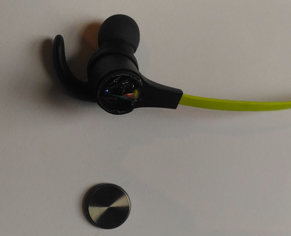
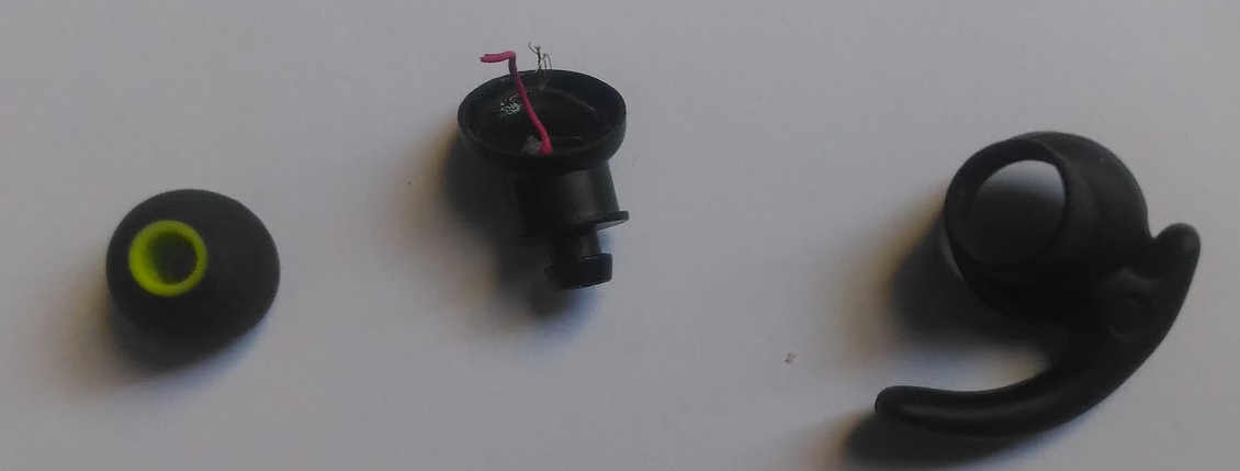
Since the product is water resistant and seems reasonably well sealed it looks like the tear down will have to be a bit destructive. Firstly the disc shaped ends of each ear 'bud' were easily dismantled, doing some gentle prying with the craft knife. A magnet was found in each disc so they can easily 'clip' together.
Just underneath this magnet revealed a small PCB for a SOT-23-5 LiPo PMIC covered in conformal coating to help with the water resistance I assume.
The opposite end of each ear bud housing were more tricky to get apart, however a bit more persuasion with my craft knife did the trick and revealed a tiny speaker (5mm diam.) attached to the two blue & green signal wires coming from the main control module.
The control module
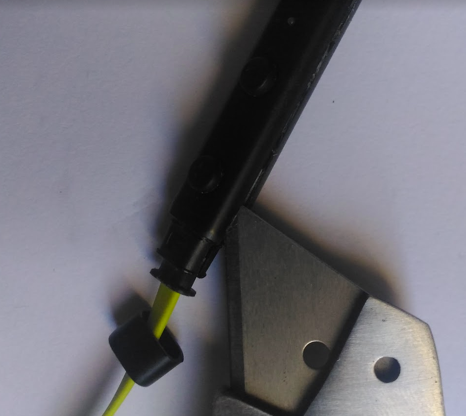
Yet again all of the housing for the control module was glued together. The two end caps could be popped off first, followed by prying open the housing with a craft knife.
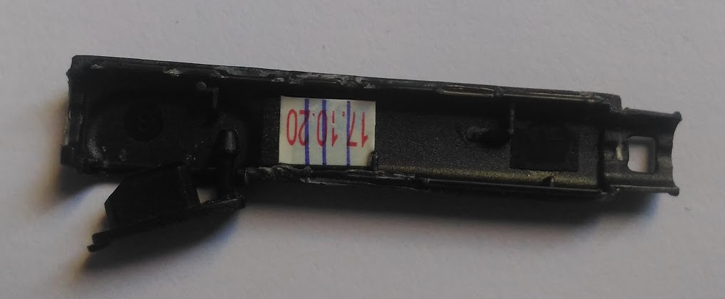
The inside revealed a very sleek tight PCB design on one side and the tactile buttons & a simple small light pipe on the other. The other side of the housing contained a small piece of marked foam pushed up against the MCU of the PCB to dampen any vibrations (which may also help the microphone performance?).
The Guts
- CSR audio SoC (https://www.qualcomm.com/products/csr8645. DS:http://www.czwtech.com/uploadfile/cfile/20121224103629171.pdf) w/ in-built LDO/SMPS
- FM24CL64B Cypress FRAM SOIC-8 (https://www.cypress.com/file/41656/download)
- Blue 2.4GHz antenna component. Likely has inbuilt bandpass filter for the ~2.4GHz. Ground stitching has been around the
- Inductors (for PS or antenna or mic?)
- A microphone with marking (2008\n7936)
- Micro-USB port
On the other side...
- R/B LED + transistor driver
- Snap dome buttons
- Potentially a MOSFET/diodes for the USB power?
The space constraint on this PCB is huge the DRC has allowed components to be extremely close to the edge of the PCB. I did often experience audible interference with the headphones whicch could be due to the smalll antenna configuration. Overall an extremely tight design and super well laid out boards.

Richie Ellingham's pages
Electronics engineer and soft robotics researcher. This is teardown territory.


