 Samuel A. Falvo II
I'm working on the DMA controller which will ferry data from the V.4 receiver into RAM. This controller is currently intended for initial-program-load (IPL) purposes, since I don't think I'll have enough resources on the FPGA to implement an appreciably sizeable ROM.
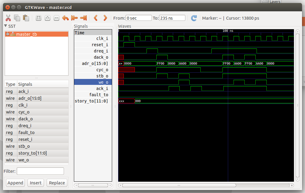
I think it's coming along well so far. Here's a timing diagram courtesy of gtkwave.
Discussions
Become a Hackaday.io Member
Create an account to leave a comment. Already have an account? Log In.