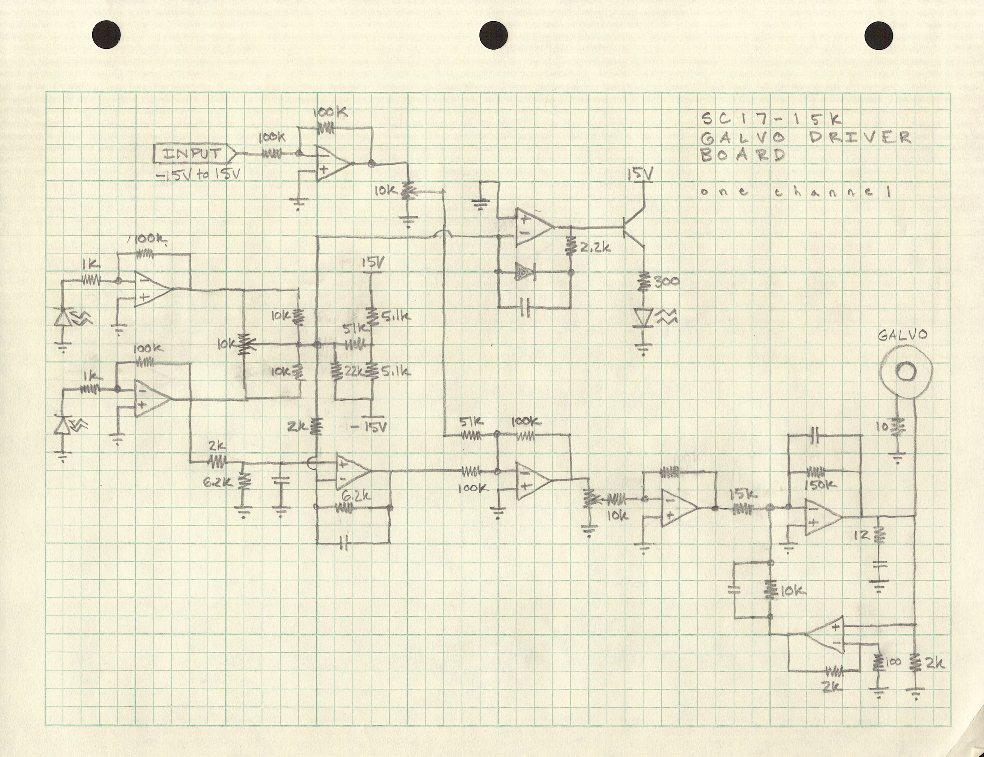
From the traced PCB that I created previously and the datasheets for the parts on the board I worked out the full schematic for one channel on the SC17-15K galvo driver:

As you'd expect, it's all op-amps. Each channel has two LM324 quad op amp chips and there's one LM358 shared between both. Then there's one NPN transistor to round out the active parts.
Preliminary analysis is: on the left there are two photodiode preamplifiers. These take the small currents coming from the photodiodes in the galvo and turn them into measurable voltages. Then there's a potentiometer to make one photodiode "count more" than the other so that bias can be adjusted out.
There's a resistor network after that which seems to be used to get a net to be ~10 volts. In the upper right that reference is used as the input to a logarithmic amplifier (the op amp with the diode). This seems to effectively be a driver for the LED in the galvo which shines on each photodiode more or less depending on the angle of the galvo.
In the upper left there's an op-amp used to buffer the input to the channel, a signal varying between -10 and 10 volts. Along with the differential measurement from the photodiodes it goes into the control / drive stage, which I haven't yet tried to analyze thoroughly. But it's safe to assume that the channel input is used to set a target which the op-amps seek using feedback from the photodiodes.
Detailed analysis to come.
 Owen Trueblood
Discussions
Become a Hackaday.io Member
Create an account to leave a comment. Already have an account? Log In.