Close
0%
0%

tinyDriver

Atmel ATtiny84 based platform to learn AVR programming.

Similar projects worth following
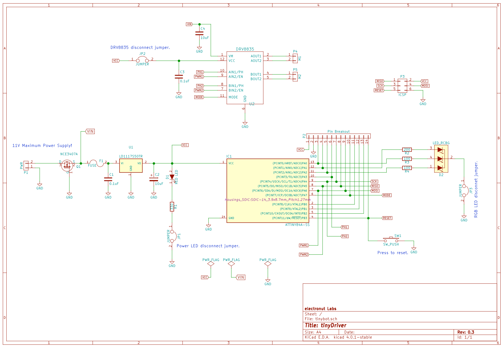
tinyDriver is a breakout board for the Atmel ATtiny84 chip, which comes integrated with a motor driver chip and an RGB LED. The idea was to create a convenient platform that can be used to understand microcontrollers in depth, by studying the datasheet and making use of the various features of the chip such as timers, PWM, interrupts, ADC, and digital I/O.

This is an Open Source Hardware Project, and you can find more details here:

http://electronut.in/tinyDriver/

I am close to launching a crowd funding campaign to manufacture tinyDriver. Please sign up below:

https://www.crowdsupply.com/electronut-labs/tinydriver

Schematic:

tinyDriver has the following specifications:

  • Atmel ATtiny84A microcontroller
  • Integrated TI DRV8835 Dual-H-Bridge Motor Driver
  • Diffused RGB LED
  • Standard ICSP header for programming
  • 500 mA PTC resettable fuse
  • Reverse polarity protection
  • 5 V regulator
  • Power indicator LED
  • Breaks out all pins of ATtiny84A
  • Jumpers to disconnect LEDs and motor driver
  • Mounting holes

Applications:

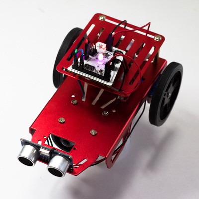
2WD Robot with ultrasonic sensor:

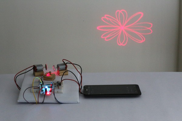
A laser display that syncs with audio input:
View all 5 project logs

Enjoy this project?

Share

Discussions

adria.junyent-ferre wrote 04/23/2016 at 12:28 point

This is an interesting project. One suggestion: in some cases one may want to measure the current fed through the driver (I'm reluctant to feed current to any motor without doing that). The poor man's option is to put a very small resistance in series with the ground return from the H-bridges and guess the load current knowing the switching state. I know this drops the efficiency of the bridge further and in this case may mess the voltage of the ground reference of the DRV8835 but if you find this feature of interest you may consider leaving a gap with a 0 ohm resistance and a few traces that may be used in case someone wants to use this. 

  Are you sure? yes | no

Mahesh Venkitachalam wrote 04/23/2016 at 13:43 point

Thank you for the feedback. Will look into this.

  Are you sure? yes | no

K.C. Lee wrote 04/22/2016 at 01:45 point

You cannot simply disconnect the DRV8835 power without disconnecting all of its input pins as there are internal diodes to its VCC pin.  There will be power leeching from I/O.

Datasheet: Section 6,

Digital input pin voltage:  –0.5 to VCC + 0.5 V

  Are you sure? yes | no

Mahesh Venkitachalam wrote 04/22/2016 at 03:27 point

OK, thanks for pointing that out. Maybe I'll remove that jumper, then.

  Are you sure? yes | no

Mahesh Venkitachalam wrote 04/22/2016 at 08:44 point

Section 9 says:

"There is a weak pulldown resistor (approximately 100 kΩ) to ground on the input pins.

VCC and VM may be applied and removed in any order. When VCC is removed, the device enters a low power
state and draws very little current from VM. To minimize current draw, keep the input pins at 0 V during sleep
mode."

So at a 5V output on a pin, the 100K draws only 0.5 uA. I have been testing loading on all 5 pins with VCC jumper disconnected and so far it looks OK.

  Are you sure? yes | no

K.C. Lee wrote 04/22/2016 at 10:51 point

I am talking about internal ESD protection, not power down. If the part could handle signals without power applied, the maximum parameter would be written differently.  They would given an actual voltage e.g. 5.5V.  The +0.5V means a diode.  

One thing you could do is to make sure that all those I/O pins are always driven low when you pull the jumper.  If they are high, then the ESD diode would conduct.

 http://www.ti.com/lit/an/slaa689/slaa689.pdf

Were any I/O pin high? If yes, Have you measured the I/O pins to the part when you do that? Measure the current from you micro to the I/O pin? Measure the voltage at the disconnected power pin?

Also read the fine print about not following the max parameters about the part might get damage?

  Are you sure? yes | no

Mahesh Venkitachalam wrote 04/25/2016 at 07:47 point

You are right, voltage from output pins is coming into the VCC pin of the IC.  I am thinking of adding AND gates on each of the 5 pins, with respect to VCC after the jumper. That should work?

  Are you sure? yes | no

K.C. Lee wrote 04/25/2016 at 08:47 point

Just using the power with AND gate can be tricky as the signal level isn't going to be well defined.

Or you an use 74LVC/AHC gates that are powered from the DRV8835 side of the jumper to buffer those signals.  These 5V tolerant series are do not have the diodes to the VCC so they don't leak power thus they are designed to be use in situations like this.

  Are you sure? yes | no

Mahesh Venkitachalam wrote 04/28/2016 at 03:53 point

I think I'll just go with jumpers to disconnect all lines. Thanks for your feedback.

  Are you sure? yes | no

JsemDroidik wrote 03/11/2016 at 08:51 point

Kudos for using Kicad :-)

  Are you sure? yes | no

Mahesh Venkitachalam wrote 03/11/2016 at 09:02 point

Thanks!

  Are you sure? yes | no

Similar Projects

Does this project spark your interest?

Become a member to follow this project and never miss any updates