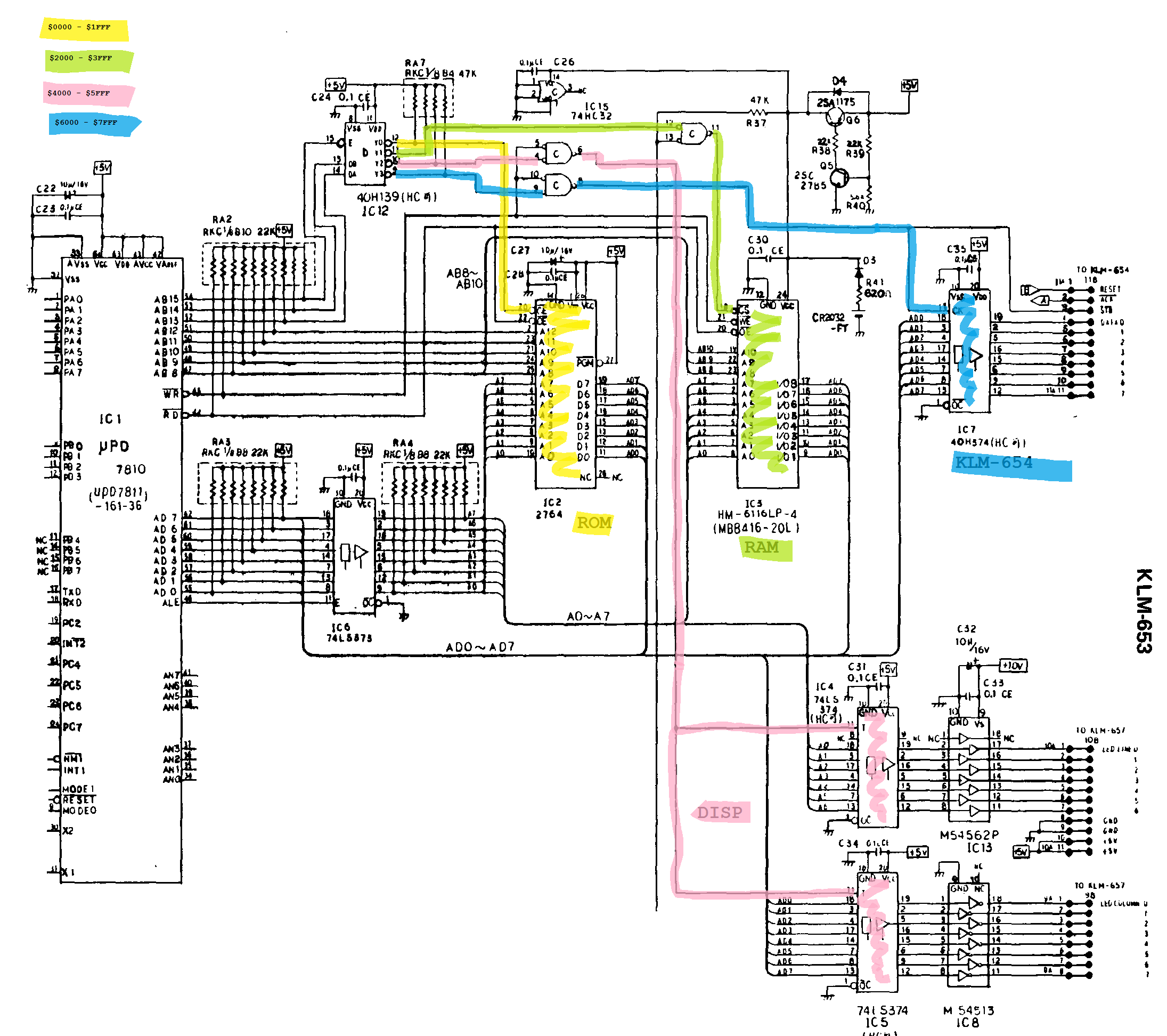
I figured out the following:
| 0x0000h - 0x1FFFh | external ROM |
| 0x2000h - 0x3FFFh | external RAM (battery backed up SRAM) |
| 0x4000h - 0x5FFFh | LED displays |
| 0x6000h - 0x7FFFh | KLM-654 |
| 0x8000h - 0xFFFFh | probably unused - setting the 16th bit high disables IC12, so no other chip is enabled - need to check this. |
The schematic below (I've removed some non critical circuitry just for readability) shows how it works:

With this information I noticed something else - there are a lot of writes to the external RAM during operation, so it means that the "working" patch values are stored there. What does it mean to me? Well I hope that there are at least four free bits somewhere (ideally four free bits per each patch) where I could store the bank number.
Right now I can try to roughly estimate what needs to be done:
- Find the place where the key presses are scanned and analyzed (i.e. only certain combinations are allowed)
- Extend it by adding one combination (e.g. 14)
- Allow to change its value within a 4 bit range (1-16)
- Store the result somewhere in the RAM
- Set the upper nibble of PB as requested.
Additionally: modify all the operations which affect PB to leave upper nibble untouched.
Looks as it could work, I only hope not to run out of memory... There are some FFs in the ROM but I don't know anything about the internal organization of RAM though. Furthermore I have this bad feeling, that at some point I will end up writing my own assembler or some kind of program which will help me deal with the jump addresses (they're going to change if I add/remove some code).
 mateusz.kolanski
Discussions
Become a Hackaday.io Member
Create an account to leave a comment. Already have an account? Log In.