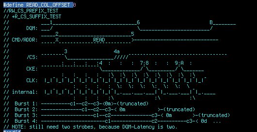
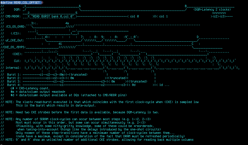
Most of my earlier timing diagrams were higher-level than reality... so I've been working on lower-level timing-diagrams. My energy's fading, so it's not yet complete... nor is what's there 100% verified (e.g. the number of clock-cycles between the one-shot signals' *inputs* and their outputs...)
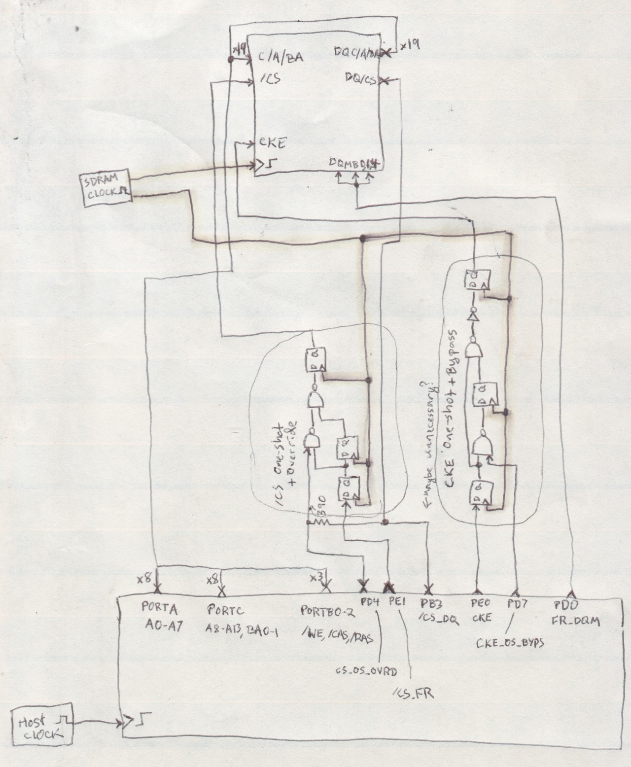
Here's the simplified diagram I worked with to code this thing up...

Key points:
- DQM must mask the data at the Command/Address DQ's for several reasons:
- At the start, there may be a burst-read in progress already or other previous operation which might interfere with loading the Command/Address in step 2
- As soon as the (first) burst-read begins, data output would definitely collide with the Command/Address still remaining on those pins as we wait to switch those (host's) pins to inputs
- Load the "Read-Burst" command (and the associated column address) to the associated Command/Address pins.
- Activate /CS changing the INHIBITED "Read-Burst" command into an *actual* "Read-Burst" command
- The data is available 3 clock-cycles later (CAS-Latency=3), but will remain masked, until we have a chance to change the Command/Address pins to inputs
- Until the next step, the Burst-Read will be repeated numerous times from the same starting-address. Each previous burst will be truncated by the next.
- Disable CKE
- The "Read-Burst" command, with /CS active, will be recognized *one* more time, alongside the first clock-edge where CKE is read LOW.
- From there-on, the "Read-Burst" command, and /CS's being active will be ignored, so disable /CS whenever ready
- The last-initiated burst-read will be immediately paused
- The "Read-Burst" command, with /CS active, will be recognized *one* more time, alongside the first clock-edge where CKE is read LOW.
- Switch the Command/Address host-pins from outputs to inputs
- Unmask the read-burst data-output to be read on the host's Command/Address pins
- DQM has a latency of two clocks during read-bursts, so we'll need two CKE strobes
- (Guess we lucked-out that step 4 allows for starting *one* more read-burst, because these two CKE strobes will result in output from the requested column (column 0) rather than one or two thereafter!)
- Strobe CKE Twice (each strobe must be no longer than one SDRAM-clock-period!)
- Skip ahead to B:
- Remask the data-output from the read-burst
- Reenable CKE
- Two clock-cycles later, the read-burst will be masked
- Switch the Command/Address host-pins back to outputs, in preparation for the next operation
- The (masked) read-burst will continue indefinitely, since it's set to burst a full page and wrap when complete... I issue a PRECHARGE command as the next operation.
Having the timing-diagram *alongside* the circuit seems to help to make things clearer.

And here it is in a bit more detail... taking into account the one-shot circuitry and the associated bypass/override signals (which may be poorly-named).

void sdramFR_readACD(uint8_t bank, uint16_t row, uint16_t column,
          uint8_t *dBank, uint16_t *dAddr, uint8_t *dCmd, uint16_t count)
{
   //Assuming the Command/Addr IOs are currently outputs:

   //Mask the data-bits so they don't write to the C/A IOs while they're
   //outputs...
   //
   //(Is this not part of the above assumption?)
   sdram_disableAllBytes();   //1

   //Activate the selected row on the selected bank
   sdram_activateRow(SDRAM_FR_DEVNUM, row, bank);


   //Prepare a read-burst (masked) starting at the selected column
   sdram_setupAddress(column - READ_COL_OFFSET, bank); //2
   sdram_setupCommand(SDRAM_CMD__READ);   //2

   //The read-burst command will execute immediately after this
   // BUT, it will be repeated/restarted with each clock-cycle
   // UNTIL the clock-cycle AFTER CKE is disabled.
   sdramFR_overrideCS_OneShot(); //3

   sdram_clockDisable();      //4

   sdramFR_enableCKE_OneShot();  //4i

   // /CS is still active
   //  Only the first, AFTER clockDisable, will be registered
   sdramFR_unoverrideCS_OneShot();  //4a


   //Set the fed-back Address/Command pins as inputs
   // (Also takes care of Free-Runner's nCS_DQ
   sdramFR_AddrCmdIO_AsInputs();  //5

   //Unmask the data-bits (will occur somewhere down the line)
   // Should be exactly two CKE-strobes later, right?
   clrpinPORT(SDRAM_FR_DQM_PIN, SDRAM_DQM_PORT);  //6


   //Assuming a CAS-Latency of 3...
   //(Right, two are necessary, otherwise still in CASL
   //  read-back floating bus from last col-assignment TESTED TRUE)
   // OR: was that due to DQM-Latency?
   sdram_strobeClockEnable();    //7,8

   //Mightaswell take advantage of the ol' bursts!
 while(count>0)
 {
   sdram_strobeClockEnable();    //9,A
   //Note that the strobe is delayed a couple SDRAM clock-cycles
   delay();

   //Now there should be data on the ports...
   //Read Back ADDRL
   uint8_t addrLval = PIN_FROM_PORT(SDRAM_ADDRL_PORT);
   //ASSUMING ADDRH and BA are on the same port... (BA = bits 6,7)
   uint8_t addrH_BA_val = PIN_FROM_PORT(SDRAM_ADDRH_PORT);
   if(dAddr != NULL)
   {
      *dAddr = (uint16_t)addrLval
              | (uint16_t)((addrH_BA_val & SDRAM_ADDRH_MASK) << 8);

      dAddr++;
   }

   if(dBank != NULL)
   {
      *dBank = (addrH_BA_val >> SDRAM_BANKADDR_SHIFT);

      dBank++;
   }

   //And tack-on the Free-Runner's fed-back Chip-Select
   //Actually, for now, this is all properly-aligned, so just change the
   //MASK, above...
   if(dCmd != NULL)
   {
      *dCmd = PIN_FROM_PORT(SDRAM_FR__CMD_DQ_PORT) & SDRAM_FR__CMD_DQ_MASK;

      dCmd++;
   }


   count--;
 }

   //Mask the data-bits so we can take back the C/A IOs as outputs
   sdram_disableAllBytes();   //B

   //But that won't be registered until the clock's enabled...
   sdramFR_bypassCKE_OneShot();  //C

   sdram_clockEnable();  //D
   //And there's a slight DQM-latency, right...?
   delay();

   //Now take back the Address/Command pins as outputs
   // (Leaving it in a known state)
   sdramFR_AddrCmdIO_AsOutputs();


   //Let's do a precharge-all just so we know where we're at...
   sdram_precharge(SDRAM_FR_DEVNUM, PRECHARGE_ALL);
}
It's, really, quite a bit of work to read/write data to the DQ's which are fed-back directly to the Address/Command pins. A *much* easier method, of course, would be to insert buffers (with output-enables) between the DQs and the Address/Command pins. But, this would also require an additional 19(?) I/Os from the host... nothing to scoff at. Then again, it would be *significantly* more intuitive, so there's that.
That "more-intuitive" system is, pretty much, what sdramThing1.0 was going for, but I ran out of I/Os (and was a bit too lazy, anyhow) to solder up DQ's for all 13 address-lines. Instead, sdramThing1.0 merely fed-back the *command* signals, and the AVR was responsible for iterating through the addresses (which only had to happen at 3/1024ths of the SDRAM-clock rate, for Precharge, Activate, and Read commands for each 1024-column page). Instead of using buffers with output-enables, I inserted resistors (much as I plan to do to whittle down the 32bits on the side-kick down to 8bits, and plausibly also for getting away with one-directional latches (such as the 74374/574) for bidirectional data-flow. For sdramThing1.0 speeds were slowed *dramatically* by, I'm pretty sure, those resistors... but if you look at them closely, I'm almost certain I accidentally used *wire-wound*. Whoops. At those speeds they weren't resistors as much as inductors. A similar set-up with a fedback-path via resistor is seen in the schematic above, where a 390 ohm resistor ties /CS_DQ -> CS_OS_OVRD, and currently runs fine at 22.3MHz.
...
On The Other Hand.... Maybe I've gotten a bit carried away with trying to make full advantage of the least amount of external support circuitry (and I/Os)... Because... it's something like 16 steps just to start a Read, similar for a Write... Without making extensive use of the burst-nature, that would *DRAMATICALLY* slow-down writing of the free-runner stuff... Ah, right, but that's only during boot, which is bordering on 3 minutes with a 16MHz processor (and, remember, 50MHz toggle-rates from a PI's GPIOs is pushing its limits)... Does boot-time really matter enough to justify at least 3 D-latches and 3 Buffers...? (or maybe resistor-networks)?
Alright, the address-jumping method mentioned previously... that'd be necessary for *all* reads/writes (including reading back of the sampled data), so that'd be a limiter *when using* the system, whereas this is only a limiter *when booting*.
 Eric Hertz
Discussions
Become a Hackaday.io Member
Create an account to leave a comment. Already have an account? Log In.