Yup, sTZero's been on hiatus for a while... life 'n such.
UPDATESs will be placed at the bottom...
Here's a thought:
SN74LVC1G123 - might just handle our one-shots... Personally, the idea of using RC timing doesn't quite sit with me, for this project, being largely variable in its sample-rate... But, maybe som'n can be done tying those R and C inputs to something like the SDRAM clock. Or maybe some other path, even with R and C fixed (e.g. at 10ns, for max-sampling at 100MS/s) as long as we can assure that 10ns pulse meets setup/hold times for the instruction-load clock-edge (when sampling at lower rates).
Dunno...
Anyhow:
https://hackaday.com/2019/02/18/inefficient-neopixel-control-solved-with-hardware-hackery/
----
2-29-20:
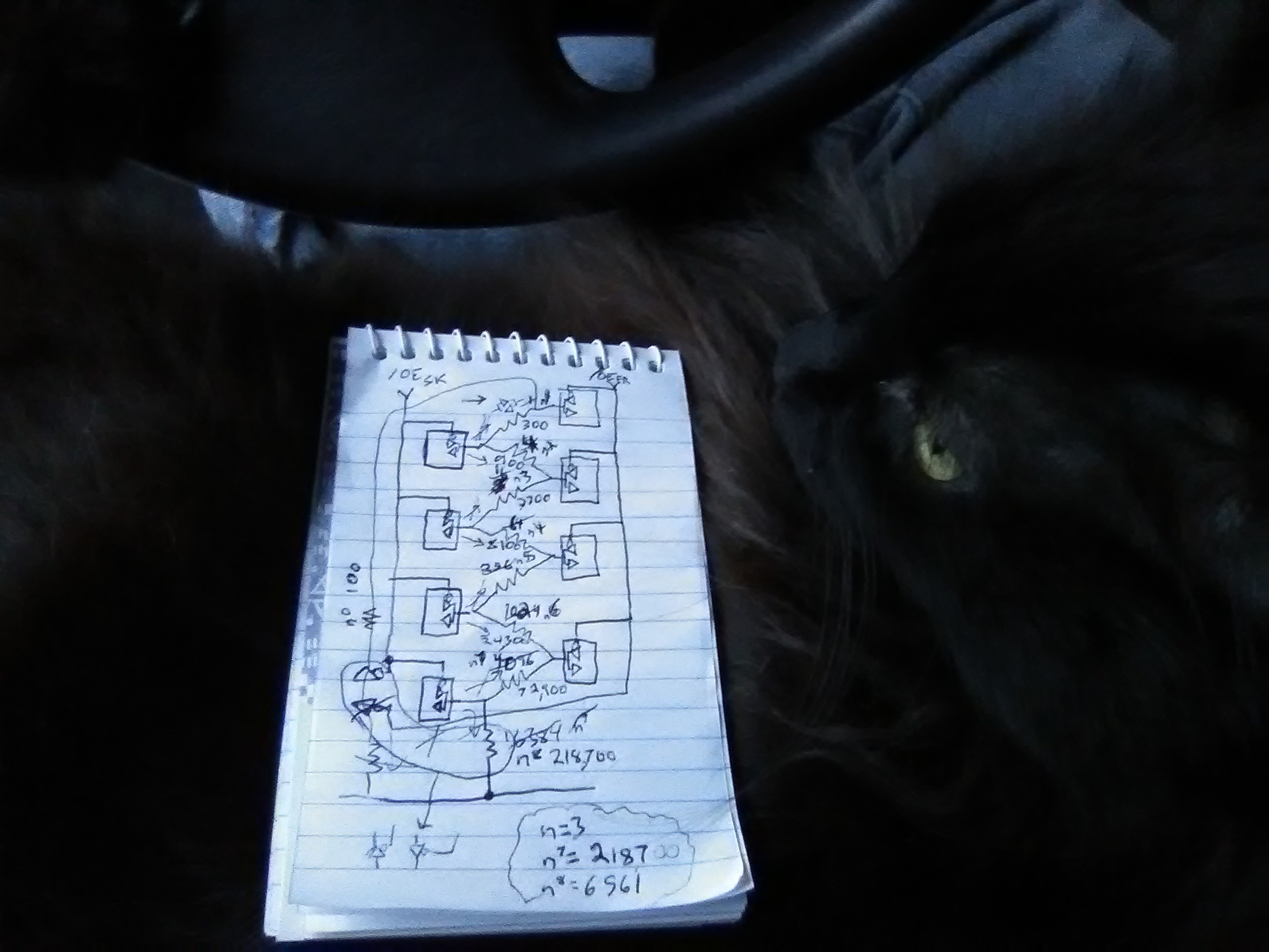
Vague idea: since trying to interface with an 8-bit bus, maybe read-back of the sampled 32bits could happen by a sort of bucket-brigade. [And maybe similar for writing the free-runner?]. E.g. read the first chip, write from the second to the first, read the first again. Thus, plausibly reducing the number of chips [loading] on the bus, and plausibly the number of latches/buffers.
Also plausible, read first SK chip to bus, read second chip to FR first chip, etc. [Overwriting FR, but can be rewritten], a sort of left-right-forward bucket-brigade. [May be more feasible; since data I/Os are a single pin, loading wouldn't be reduced much if B4->B3->B2->B1, but would if B4s->B3f, B3f->B3s... erm, no...]
BUT: B4-/\/\/-B3-/\/\/-B2-/\/\/-B1-/\/\/-Bus... hmmm. Only not-so-much, *maybe* since all SK chips [and all FR chips] use the same command signals [ [all chips reading/writing simultaneously] I Wonder, since read-commands and write commands take a different number of clock cycles, maybe a read's data would linger long enough to be registered by a write, hmmm. Could be handy elsewhere, too [copying FR commands/NOPs from bank to bank?] ].
BUT: B4s-/\/\/-B3f-/\/\/-B3s-/\/\/-B2f-/\/\/...B1s-/\/\/-Bus... wouldn't have that limitation [read from SK, write to FR simultaneously should work]
[Of course, B4s=1, B3s=0, B3f=0.5... hmmm.... resistor values increase left to right? Diodes? Buffers, of course, but then more control signals /OE, when sampling, no?]
Ideally, would also reduce the number of control signals necessary to select which byte to read-back [knowing they'll always be read in order]... a sort of byte-wide shift-register.
---

8 devices attached to a bus with only one buffer [two slightly preferable]. A shift-register, of sorts...
---
Ahhhh...
But this overwrites one side's data with the other's.
It works[?], in this case because the Sidekick's data is loaded from the sample inputs *not* from the bus, thus Read-only, from the bus's perspective. Whereas the Free-Runner is [or could be] write-only from the bus's perspective.
Sample-data can be destroyed upon read-back AND when writing the Free-Runner. Free-Runner data can be shifted back in during either process. Weird.
The resistors could be replaced with buffers with /OEs tied directly to the other /OE's... I spose that'd be easier to design. And still no extra control signals necessary.
But I'm a bit fixated on using passives; making use of the circuitry inherent to the devices... dunno why. And resistor-nets are a *tiny* bit cheaper, no?
----
And more pondering... I think it requires a DQ latch to store the new FreeRunner data to be shifted in while shifting the data from the SideKick into the other FreeRunner registers... because, at that same time, the last SideKick register is also outputting to the bus [so can't contain the new FR data simultaneously].
Here we have a new dilemma... with another shift-reg comes another control signal [though "strobe" may be necessary elsewhere anyhow]. So, another option is to sacrifice 8 bits of sample-inputs to use as that register. Wastes a lot of memory and brings the sample inputs down to 24 from 32... but, easier to program, faster to read/write, fewer chips, and likely fewer control signals. Definitely a consideration... could be, for instance, an *option* with a few jumpers on a PCB, or could be a simpler design for hobbiests to implement on their own... every chip and wire makes for more points of failure [e.g. noise, propagation delays, etc.] So, for e.g. a first run/prototype/breadboarded weekend project/kit it may be a good option.
----
LOL... these aren't merely registers, they're RAM, with MEGABYTES of addressable storage locations.
I could *easily* sacrifice a single page [or even a row] for nothing but shifting/shuffling data, and not even care what's overwritten in that "temp" page.
And here I was worried that reading back the sample data would be destructive to the "program," and thus would have to rewrite the program memory while reading the sample memory.
LOL MEGABYTES to work with, here. Sheesh!
---
On another note, because of "burst" reads/writes, I think I can copy an entire row [from one bank] of sample data [256-1024 bytes, depending on the chip] during each "shift" operation.... and likely do-so at the full SDRAM speed of, say, 100MSps. So actual read-back into the computer via the bus will be pretty much the limiting bottleneck, *not* the fact that the data has to be copied 7 times!
Further thoughts on this path over at #Memory Shift
https://hackaday.io/project/170172-memory-shift/log/174383-overview
---
Been meaning to link this... I've certainly pondered sdramThing's ability to be used as a processor... I think I've other links/thoughts on the matter in other logs, at #sdramThing4.5 "Logic Analyzer" , on my website [should be in the external-links at this main project-page], and/or in the source-code. TODO maybe someday work on consolidating such notes by topic?
https://hackaday.com/2020/02/20/a-turing-complete-cpu-from-ram/
 Eric Hertz
Discussions
Become a Hackaday.io Member
Create an account to leave a comment. Already have an account? Log In.