 Eric Hertz
This log from #sdramThing4.5 "Logic Analyzer" (https://hackaday.io/project/4159/log/33427-cke-well-shit) was the turning-point in whether this venture would be even remotely possible...
Before, precision timing was necessary... Once a Write command was invoked, the same pins used to send that command would then need to be switched to the data to be written, then a strobe on the "Data-Mask" bit would allow that data to be written to a memory location. This would be dozens of SDRAM-Clock cycles later... which means it would write whatever data I loaded to a memory location dozens of locations *after* the one commanded by the Write command. Math, and an exact number of CPU cycles, was necessary to determine which address to request in order to write to the *actual* address you wanted. Read-back was similar.
So, CKE... I dunno why I didn't consider it an option before, but for whatever reason, I didn't. Which apparently made life quite a bit more complicated than it needed to be. For sdramThing4.5, FOUR one-shot circuits were necessary, nevermind the Assembly-based Read/Write functions, and more...
So I've been drawing some timing-diagrams, and reading the specs more thoroughly... it gets real fun reading those specs, as they sometimes seem a bit conflicting from section-to-section, but eventually I think I pieced it together.
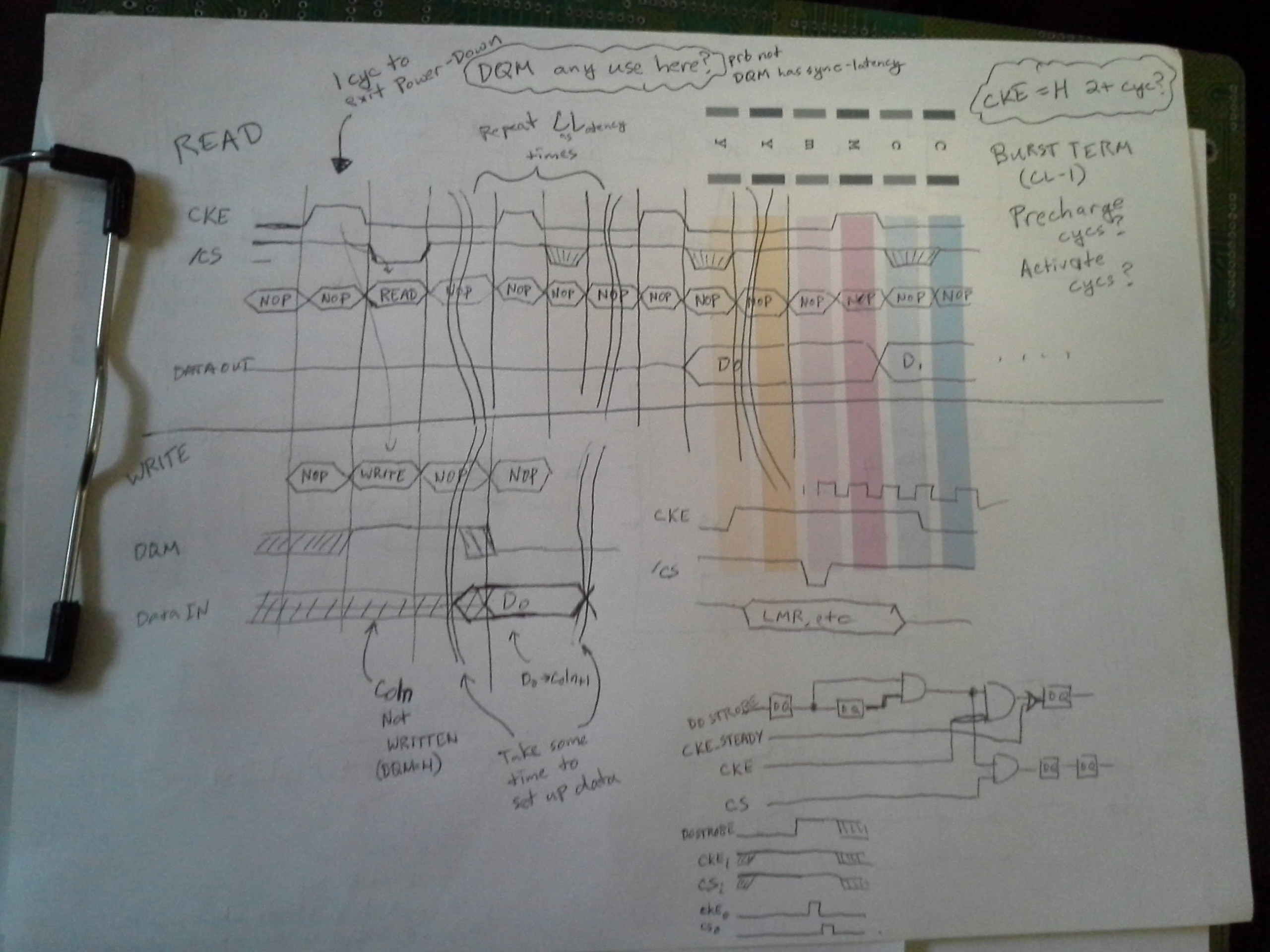
The key-ingredient, here, is that Clock-Suspension (via CKE) is only possible during the Read and Write bursts. (which is fine, that's where it's needed most). An alternative is "Power Down" mode, which can only occur alongside a NOP command (or Command Inhibit, where /CS is inactive). So that means it's not possible to set up the command (and, more importantly, the /CS pin), then "strobe" CKE.
So, that means that BOTH the CKE pin AND the Chip-Select pin need to be "one-shotted." Further, in most cases where CKE will be strobed, only the *next* command is accepted... So CS must be active in the *next* clock cycle after CKE.
OK, so, a one-shot circuit wherein CKE occurs first, and CS occurs second. Really, that's only one extra latch, to add a delay... a really short shift-register.
Then there's the factor of certain commands which can't be "powered-down" nor "clock-suspended" immediately-thereafter... E.G. the Precharge command (which closes a "bank" of memory) takes a few clock cycles to complete. In that case, CKE needs to remain active until it completes.
Here we can take advantage of the fact that when /CS is inactive, it doesn't matter what's on the other command-inputs. So, first, we'll start-up CKE, then load the command (with /CS inactive), then strobe/one-shot the /CS active, then eventually disable CKE again (putting the device in "Power-Down" again). The only piece that's timing-specific is just that /CS must only last for a single SDRAM clock-cycle.
Oh, right, so what does the CKE-strobing give us with Read/Write...? Well, in the case of Write, it means you can load the write-command (with /CS active, but disabled through the one-shot circuitry), set up CKE to strobe, then toggle the one-shot circuitry. That'll strobe CKE for one clock cycle, bringing the SDRAM out of "Power Down" mode, Then it'll strobe the /CS pin for one cycle, starting the "Write" operation... Oh, I forgot to mention that the Data Mask must be enabled before /CS is strobed... Then... That first address will not be loaded, but the clock will be suspended immediately after the write-command is issued. Now you can take as much time as you want to load up the data to be written, deactivate the Data-Mask, etc... Then when everything's all ready you can strobe that CKE one more time, and the data you just loaded will always be stored at one address after the one requested (without messing up data at the one requested).
EASY. Seriously... It was *way* more complicated the old way. And timing is utterly moot... Alls it takes is a handful of latches (and, realistically, I probably went a bit overboard, just making sure everything's perfectly synchronized without worrying about gate-delays), and a few gates.
Here's the initial proof-of-concept for the one-shot circuitry. Another difference between this and that of sdramThing4.5 is that now instead of using separate one-shot circuits for each signal, I use *one* that activates all the other signals. This is good 'cause who knows exactly *when* the signal will transition (WRT the SDRAM-clock)... If two signals needed one-shotting during the same SDRAM-Clock cycle, but occurred *right* at an edge, one might one-shot in one clock cycle, while the other might occur at the next. Here they're perfectly synchronized, regardless of when the "DO_STROBE" signal occurs WRT the SDRAM-Clock.
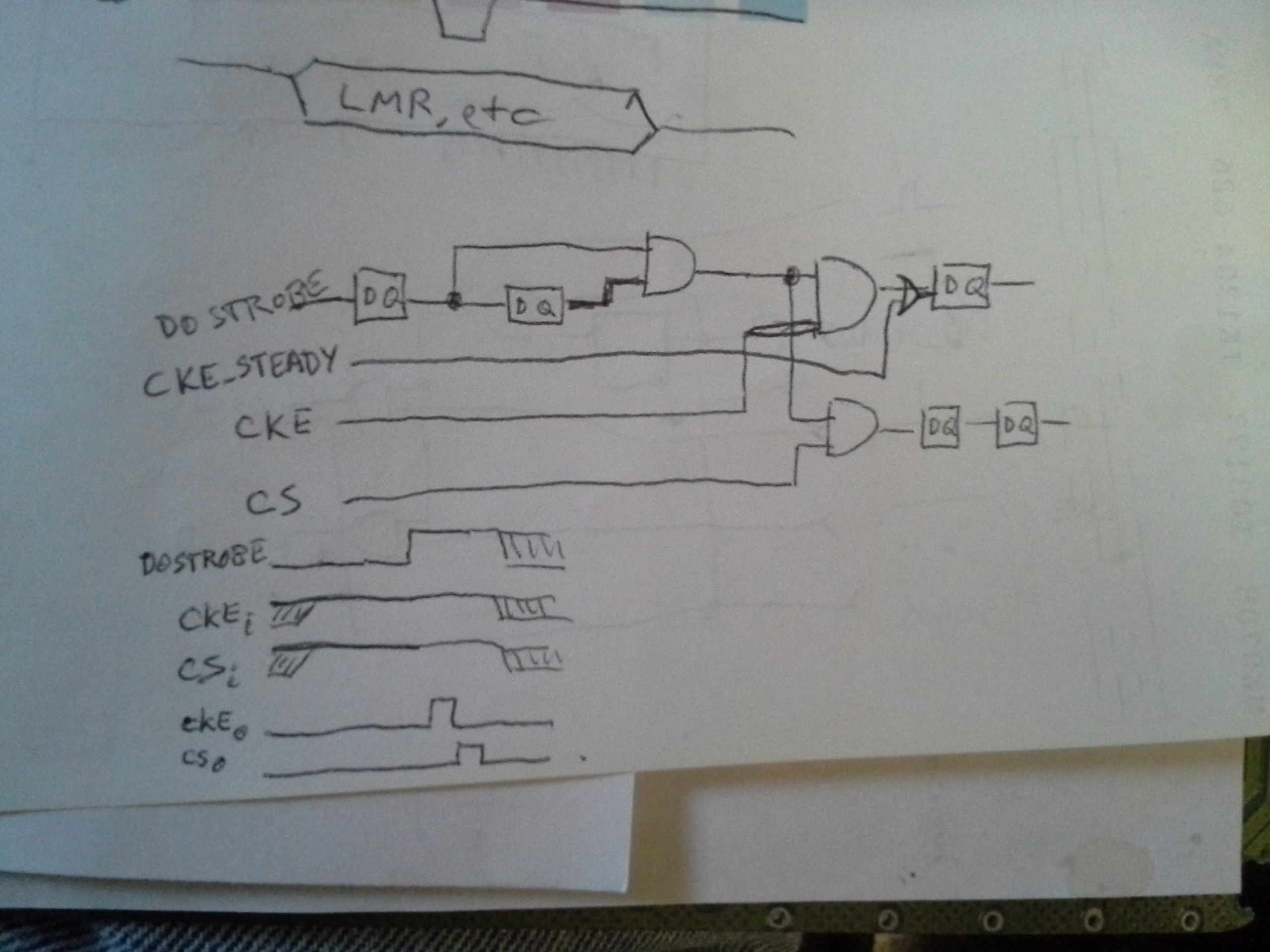
And here's the read/write timing diagrams... Note, another nice feature of this CKE strobing is that it's *really easy* to write to or read from sequential addresses in a burst...... Too easy, really...
Yahknow, I think where I got into trouble with sdramThing was that I was thinking about ddrThing quite a bit as the next iteration...
-------------------
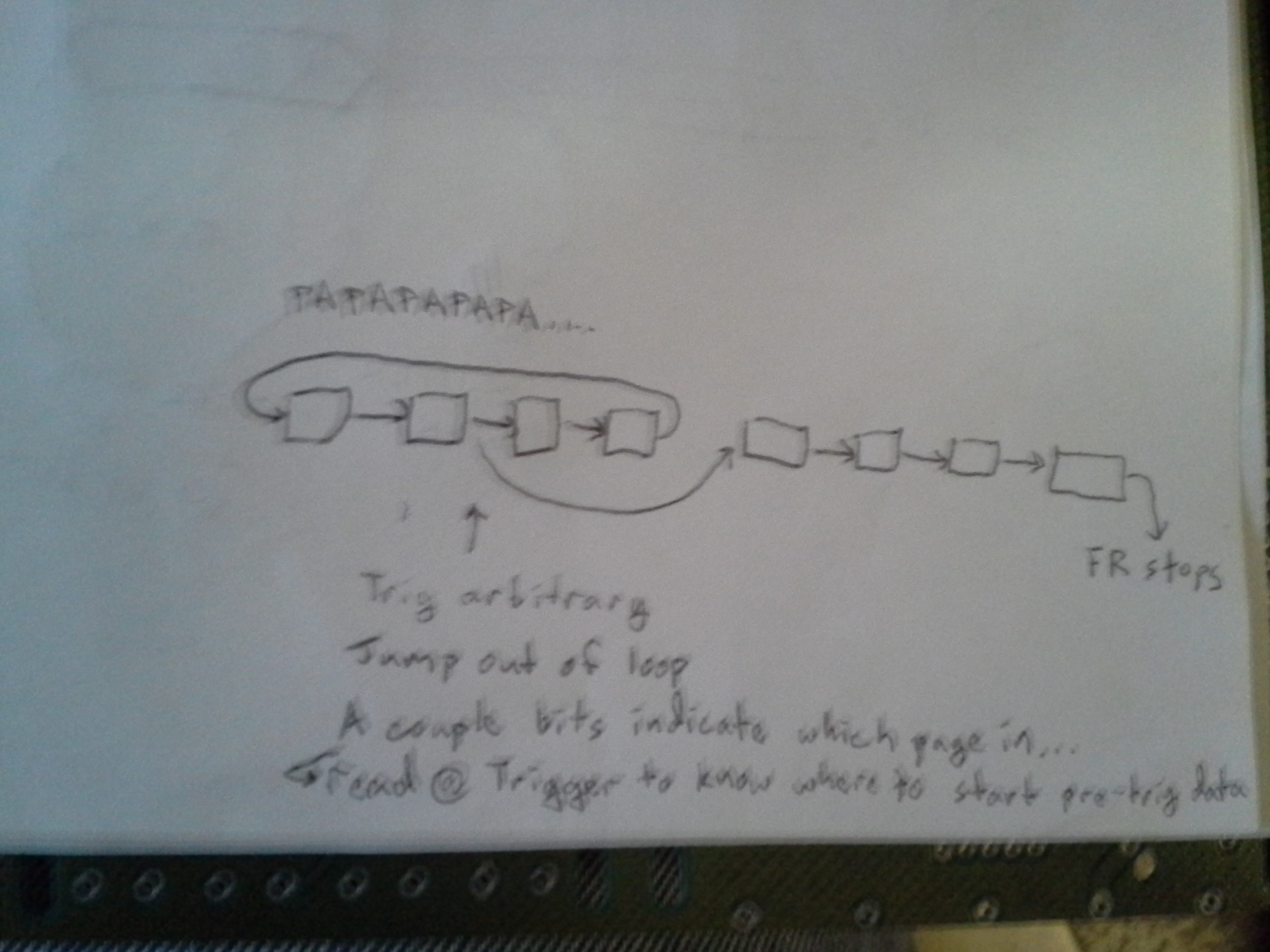
Anyways, Another thought for down the road is about how to trigger the sampling... An external trigger is one thing, a trigger from the Pi is another... but neither are particularly precise. It would be nice, I think, to have a circular-buffer running at the beginning... I think I've figured that out, as well...
"PAPAPAPA" means load the data-locations with Precharge and Activate commands for *all* the pages in the memory. This is a technique I figured out back in sdramThing2.0-ish that allows for "refresh" of the memory *while* Free-Running. It's possible to do a burst-read on one bank, and precharge/activate the other three banks at the same time.
------------------
And some other thoughts... How much do I want this to be universal...? Should it work with dang-near any SDRAM DIMM that might be inserted, or should I consider hack-jobs a worthy-goal...? E.G. sdramThing4.5 could easily grab some extra bytes from the "Free-Runner" by merely "popping" a chip-select pin and rewiring it to the "Side-Kick"... bumping it from 32 simultaneous bits-sampled up to 40. Use an ECC DIMM, and then you've got 48. But, of course, doing-so means adding additional latches/buffers for read-back. Maybe they'd be unpopulated on the PCB for hackers' delight.
Another thought: It's also possible to bump it down to e.g. 8-bits wide, but then 4x the samples per channel... If that was the *goal*, a whole bunch of latches/buffers could be completely removed from the circuit... but sampling a shitton of bits simultaneously seems like a worthy enough goal to keep 'em in the circuit. But is it worthwhile to make switching between 8 and 32 a possibility...? hmm. That'd probably require some *more* buffers...
Then there's some other thoughts... Does it make sense to be able to read-back the Free-Running commands...? Doing-so would require some buffers, since we're short on pins. The only reason I can think is for verification-purposes... to verify the data's been written correctly (which is definitely useful during debugging).
And, what about *writing* to the sample-memory...? Again, more buffers.
And, finally, what about the actual interface-side-of-things...? Should I contemplate what will be hooked up to this, or just leave it as "LVTTL-compatible"... At some point it'd be wise to consider things like opto-coupling. And, then, there's the "oscilloscope"-factor... if we're attaching ADCs to these bits... how far are we going with this...? Should it have scaling for up to 250V input? Amplification for 50uV?
Wherein I'm a bit overwhelmed.
Discussions
Become a Hackaday.io Member
Create an account to leave a comment. Already have an account? Log In.