 Eric Hertz
(Update 2: Now 6 of 7 DIMMs from various manufacturers have been tested-functional. The 7th...? Not sure yet... too much current-draw?)
(Update: Running! AVR: 16MHz, SDRAM/One-Shots: 22.3MHz)
So the setup: The AVR is now running on a separate crystal-oscillator than the SDRAM (and its one-shot circuitry connected to /CS and CKE).
The AVR's set-up to simulate a slow "asynchronous host" by inserting lots of NOPs between all signal-transitions: especially, e.g. /CS and CKE outputs are active for something like 4 AVR clock-cycles.
When the AVR's clock-source is connected to the SDRAM (and one-shots), the circuit works without a hitch... 100% read/write verification.
When the AVR's clock-source differs from the SDRAM's, I get read-write verification-failures of something like 10%... I've tried various combinations of a half-dozen crystal-oscillators (on both the AVR-side as well as the SDRAM-side)...
One of the more-interesting results is that there are even failures when the AVR's running at 16MHz and the SDRAM/One-Shots are running at 8MHz... (again, all signals output by the AVR are running at about 4 AVR clock-cycles per transition, so no risk of one-shot signals being missed, right?).
This one's interesting, I guess, because it means that the clock-signal-routing to the One-Shots and SDRAM aren't likely *the* (though, maybe *a*) problem, since when both the AVR and SDRAM/OS are running on the same 16MHz clock, the results are 100%. (Note also, I've resorted to using a clock-fanout chip with a PLL... the CY2305)
So, LOTS of experiments, and lots of circuit-revisions. including:
- Originally used a 74HC74 for the CKE one-shot, but its clock input seemed much more sensitive than the 74AHC574, so switched all one-shots over to that chip
-
Due to supplies: used NANDs
(rather than the AND and OR for the CKE and /CS outputs,
respectively)
- Doing-so means daisy-chained gates, and different delays for different edges. In one case there's one gate-delay for the one-shot output activating and two gate-delays for its deactivation (meaning, it's *possible* its output could be registered *twice*, as it's wider than one clock-period)
- Instead, moved each "stage" inside a latched-stage... should result in the exact same delay regardless of the edge. (However, note, it wasn't a problem when the AVR and SDRAM/OSs were synchronized, and the one-shots' inputs are latched from the AVR with the SDRAM/OS clock...)
One guess, I suppose, is that with separate asynchronous oscillators, there's probably a time, from time-to-time (even if both oscillators are 16MHz, they differ *slightly*, right?) when an AVR-output transition occurs *right during* the set-up/hold times of the latch feeding into the one-shots...
In which case, I suppose, it's plausible, maybe, that somehow possibly the data in gets garbled, possibly. OK, then... So, say it's just *missed*, then it'd be picked-up on the next clock-cycle. I don't quite see it somehow resulting in a problem. It's not like somehow it's going to latch a value *other* than 0 or 1 to its outputs... right? Though, I have tried adding an additional latch beforehand, with no change.
The other theory, which is a relatively new one, is that the transitioning of the *other* signals occur at random locations in the SDRAM/OS clock-period... Except, a large number of them change simultaneously. These are the Address and Command signals (excluding /CS and CKE), as well as DQM. So, maybe, if there's enough cross-talk between all those and either /CS or CKE (into the SDRAM), then maybe those transitions are causing false-positives.
An interesting result: The verification-errors appear, by and large, to be returning values from nearby address-locations. E.G. if I read column 1, when there's an error, I seem to be getting the data (that should've been) stored in column 0 or column 2. That would make sense if CKE single strobes are being registered twice... E.G. during WRITE, it would be writing the same value to *two* columns. During READ it would be briefly activating the expected column, then the second-CKE would burst it to the next. Thus, I think I can imagine why I'm getting-back *both* the "prior" column AND "following" columns in some circumstances.
(Wherein I ponder whether it'd be a worthy experiment to have one-shots that output a *half* clock-period pulse... hmm)
Also, interestingly, Depending on which direction you write the columns (0->255, or 255->0, note that I'm writing all columns first, then reading them back), the data-errors seem to lean more heavily toward "prior"... which, again, would seem to confirm double-writes. But, the errors aren't *limited* to that, so... more to be contemplated. Some errors appear to result in no write at all, and some seem to be the result of reading floating data-lines (as somewhat verified by the fact that the data read is identical to the value last-written to that port, NOT to the memory).
(Wherein I ponder: ... no not quite there yet...)
OK... I also thought I was running into a clock-problem, like in the previous "scare"... and did a bit of looking into that (including finally soldering down the "receiving"-end shields to ground)... but, again, it's working 100% consistently when using a single clock for everything, even at much faster clock-rates. And, now, we can't blame loading on the various output-characteristics of my oscillators, because that feeds into a clock-regenerating fan-out chip (with PLL).
Reading back the last two paragraphs: Wait, CKE-strobing is only relevent DURING the read/write procedures, *everywhere else* CKE is always active. HMMM... Wherein I was almost convinced that *no other* signals change during that time, but that's not right. That's right for /CS, which is *always* ... EUREEKA. Friggin' /CS is *always* one-shot. My timing diagrams are wrong!
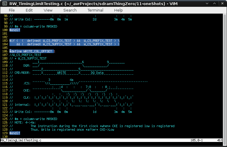
That's (roughly) what's output by the AVR... Except there are random delays between each step (1->2, 2->3...)... Even CKE's pulse at 7->8 is (now) delayed across several clock-periods... in order to test out those one-shot circuits. BUT
This design requires /CS to be active *before* AND *after* CKE's transition low at 4.
Note that, by-design (or at least per the spec-sheet I read) the command registered at the same time as CKE is registered low is VALID, but all commands thereafter (when CKE is low) are ignored, thus /CS is irrelevent after the first clock-edge after CKE goes low. Thus, I know exactly how many internal clock-cycles occur between the last-registered WRITE command (the rising-edge-clock after CKE goes low, at 4) and the CKE strobe.
BUT: my /CS one-shot circuitry doesn't have a bypass! So, it's registering only *one* WRITE command, *long* before CKE's going low... AND completely-arbitrarily, when running at different clock-speeds.
DUH.
So, when the AVR's in charge, with a sync'ed clock, we don't have a problem because there's a specific number of clock-cycles between /CS going low and CKE's going low. AND: Read-back works quite similarly.
Friggin' days, now, I've been fighting this one...
This mighta been found much sooner if I knew exactly which column is column 0... Maybe I should work on that soon... Then again, this fix pretty much guarantees it, right? (that's what I thought last time!)
Discussions
Become a Hackaday.io Member
Create an account to leave a comment. Already have an account? Log In.