 Sergey
This is how it looks like in a working prototype mode.
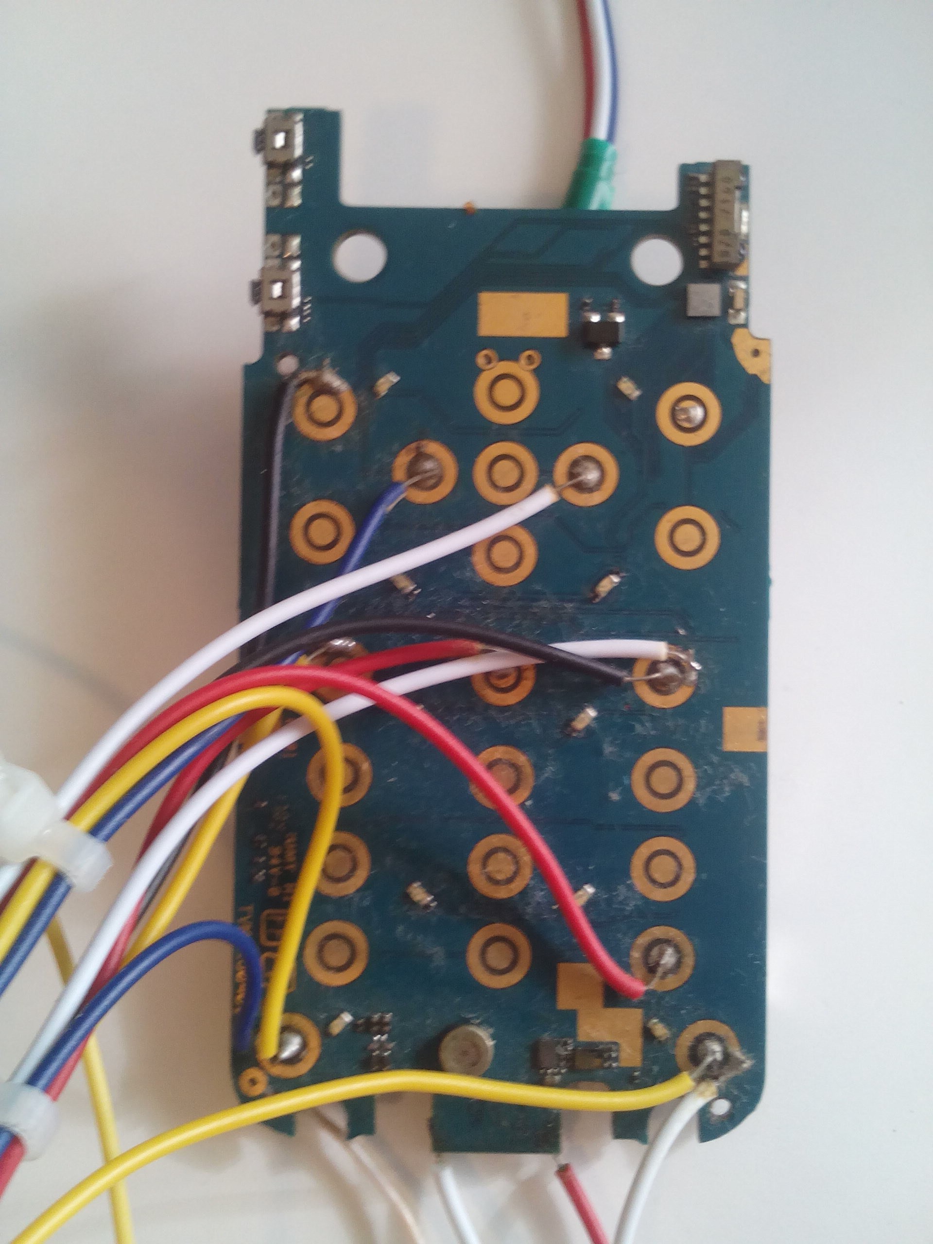
This is a board of SonyEricsson Z530i with attached wires to rows and columns in the keypad matrix
You can read about keypad matrix more for example here
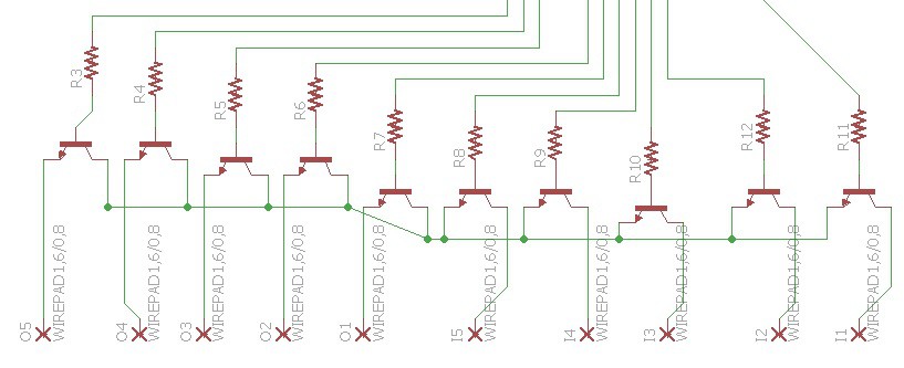
In order to reduce amoutn of MOSFETs I need to manipulate this matrix, I've decided I can use a single wire for all "columns". Because phone keypad chip already knows which column it listens to right now and the rest are silent at this particular moment, so they cannot interfere. That why a schematic for my MOSFETs is the following (In - input column, On - Output row):
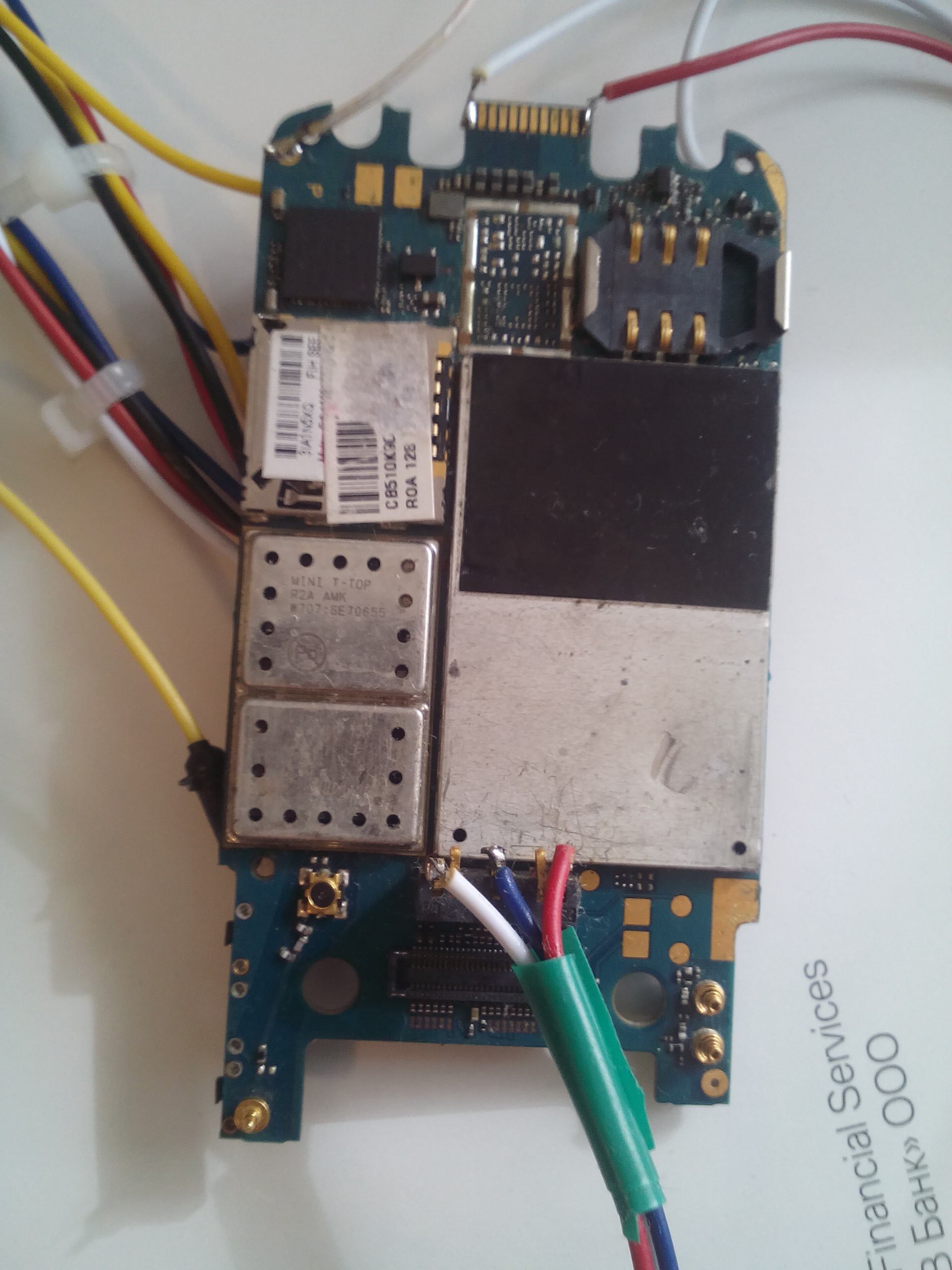
Here are some picture of the back side fo the phone PCB (battery and charing wires are soldered)
Here is the prototype PCB with wires from phone going in and some supporting circuits such as battery power metering
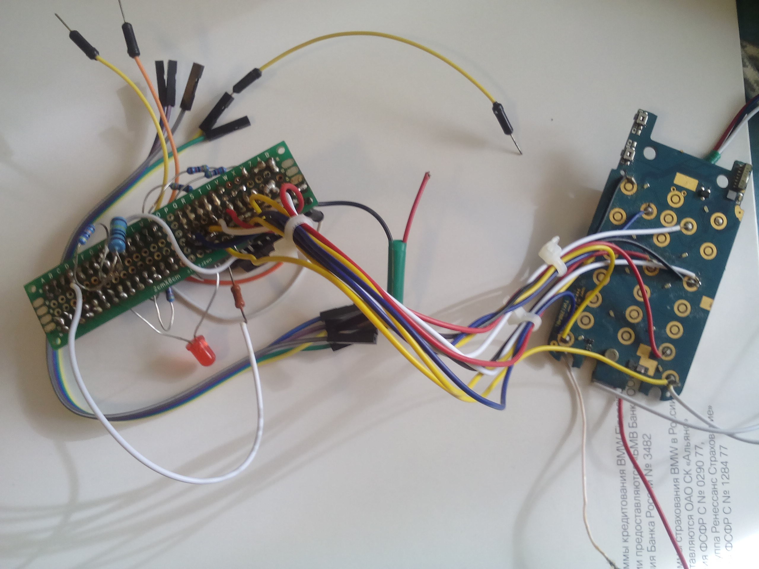
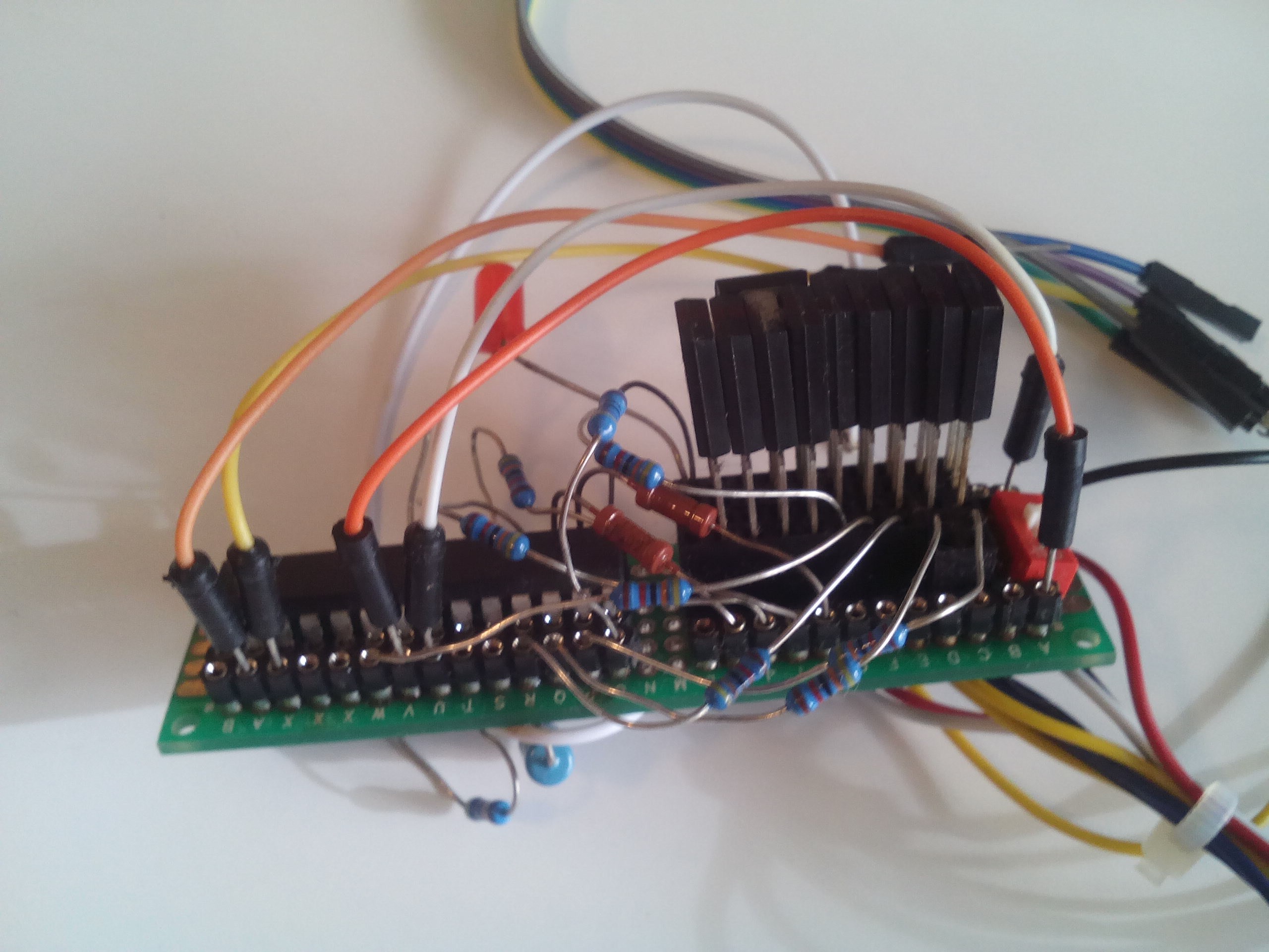
Here is the other side of the PCB. Array of MOSFETs which are connected using resistors to the Atmega328PU pins. Atmega chip is bootloaded with firmware to use internal oscilator, so that I don't need to have a dedicated circuit for it.
I'm going to share Egale files for the integrated PCB when I test that it's working correctly.
Discussions
Become a Hackaday.io Member
Create an account to leave a comment. Already have an account? Log In.