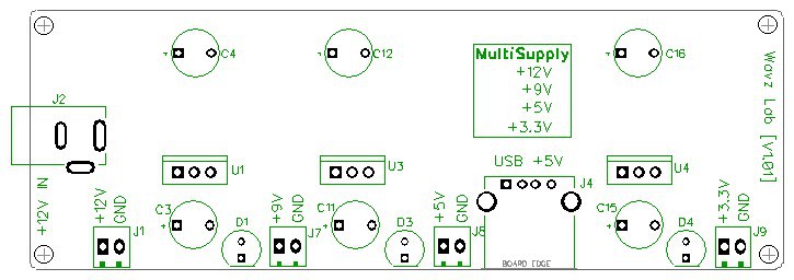
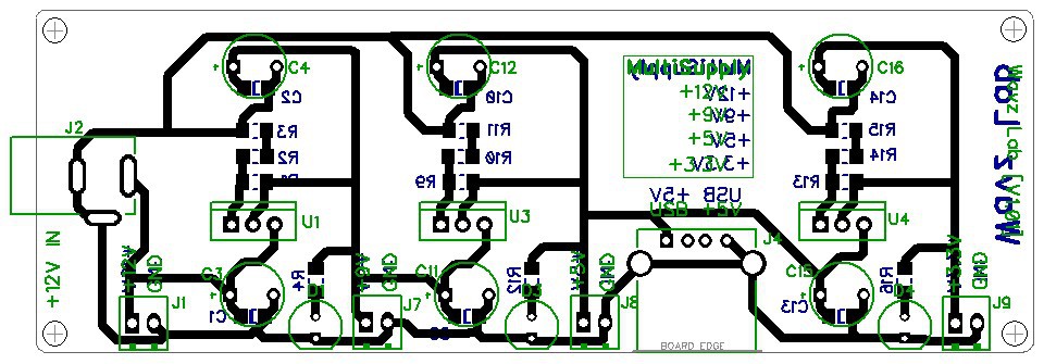
Well, As stated earlier, My goal is to design board such a that any DIY PCB etcher can do.
So, I gave special preference to net classes, by making all of them to 1 mm. [thicker traces are best in Iron based toner-transfer method]
I choose DipTrace PCB tool to design the board, It's really an easy tool to work with.
Speaking of placement, I followed K.I.S.S.[Keep it Smart & Simple] rule, and tried well for it.
Placement:

Routing:

 Amar Potdar
Discussions
Become a Hackaday.io Member
Create an account to leave a comment. Already have an account? Log In.