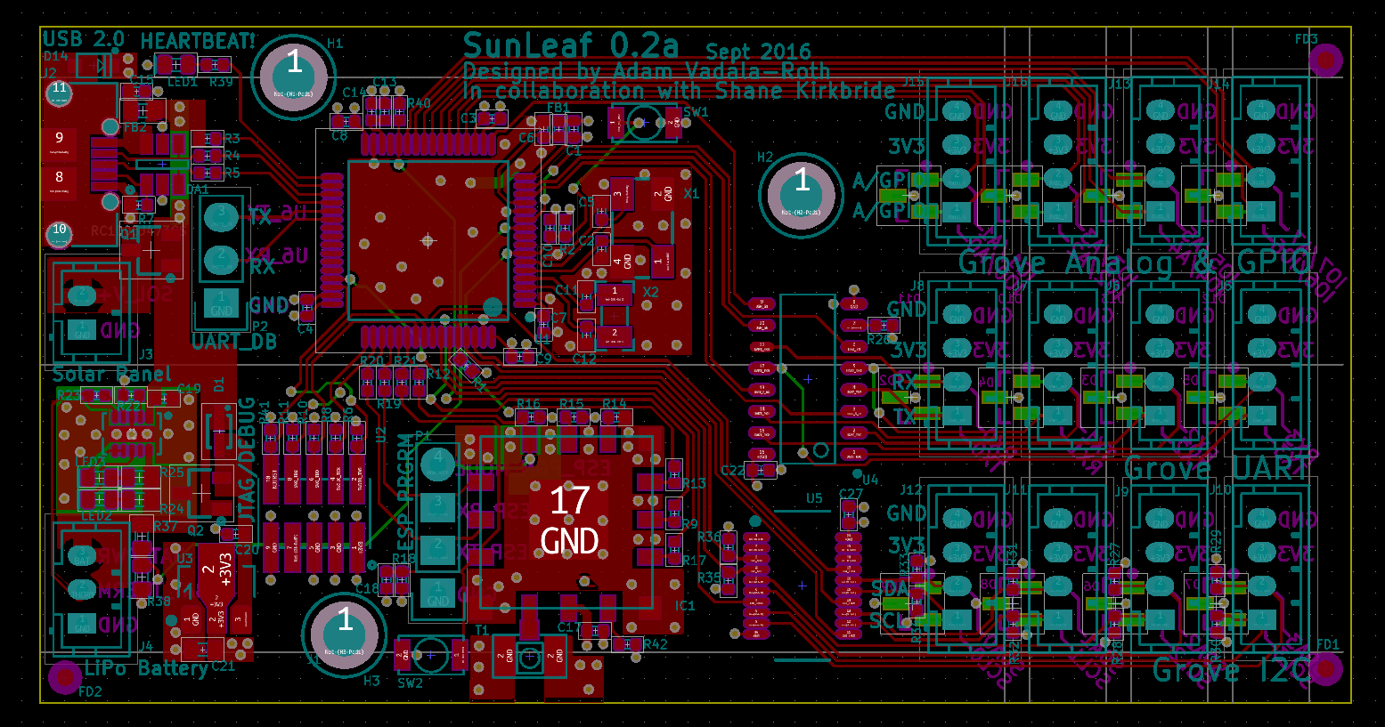
So its been a short while since we discussed SunLeaf hardware. there's actually be a lot done since the last update readying the PCB ready for fabrication. In the last few weeks I have been slowly cleaning up the PCB routing, eliminating design rule errors, and making sure all reference schematics were followed.
Most of the work though was spent getting the board ready to fab with KiCAD and its built in plotting tools. I wanted to put the board through serious design rule checks to ensure that it fabricates without any issues that could cause problems down the line. Also while retooling the boeard and squashing DRC violations, I added three M2.5 mounting holes, so that a new 3D case can be easily designed and 3D printed.

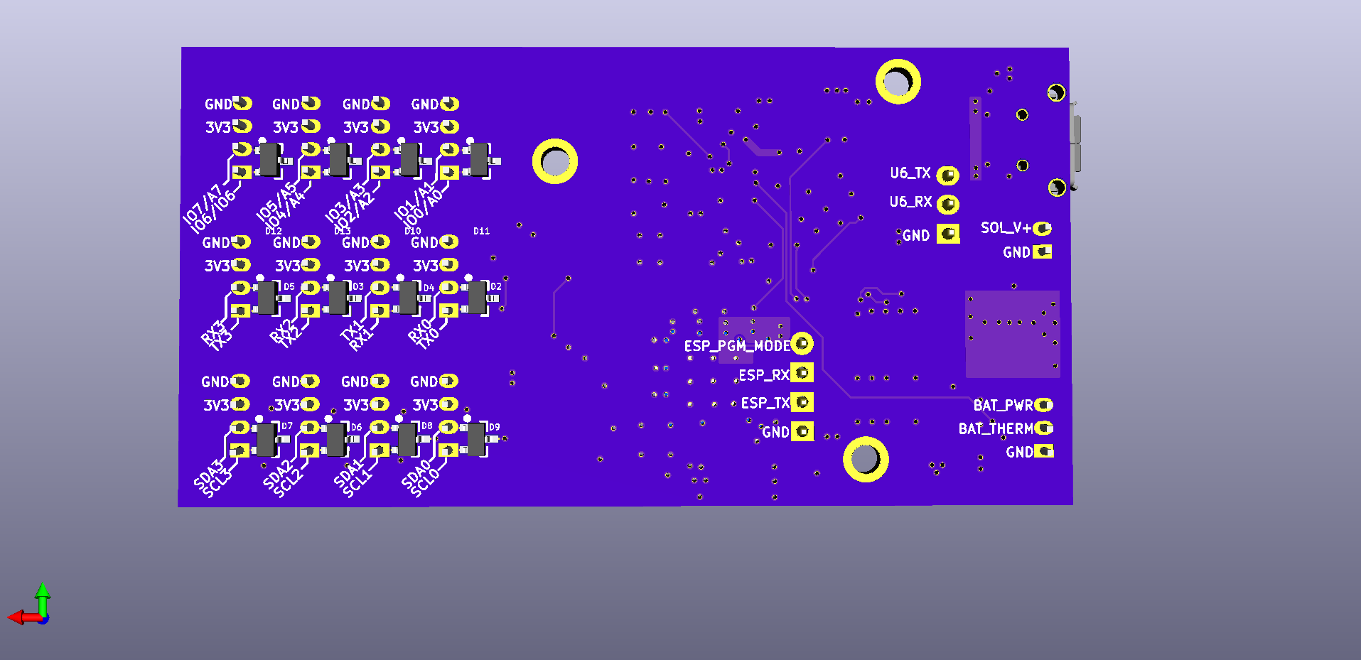
Another I updated was labeling, and fiducials. The board feature a lot more labeling of pins and and connectors. Everything from the sensor inputs, battery, solar, USB. JTAG is labeled, bottom side of board features labeling of each pin. The fiducials are for automated assembly, so pick and place machines know the orientation of the board when placing components as sometimes the board can be rotated by the machine during assembly etc. Another fix was adjusting all copper pours that re nearby each other to not overlap and to pour with the right amount of clearance so as to not violate the design rules. This sort of function is typically handled automatically in a professional design tool like Altium, not to say that KiCAD is not capable of professional work you just need to know what you are doing and do a lot of things manually, not that much of a problem, those of use that use a lot of open source software are used to these sort of things. More of the fixes include cleaning up of ESP-09 module, adding a larger ground pour beneath it and adequately stitching to the internal ground layer. The internal plane for power has also been cut beneath the antenna connector to cut down on interference with RF transmissions. Another update include a header to connect to UART6 on the STM32 for debugging over a USB serial converter. The JTAG connection was also cleaned up and a pullup resistor added to the JTAG reset signal, in the original SunLeaf the button reset pin was used for both JTAG and user reset, while it worked it was not the correct implementation and has been since corrected. BOOT1 pin has been pulled high with a 10K pullup and is now driveable by the ESP this correction is for the OTA programming functionality. On the ESP-09 CH_PD has been pulled high for ensure proper operation, deciding whether or not to have this controlled by the STM32 yet.
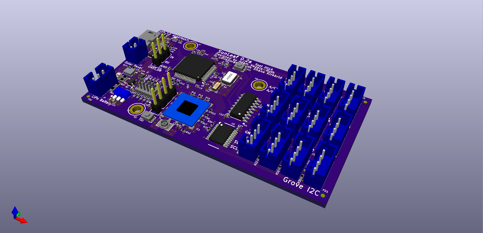
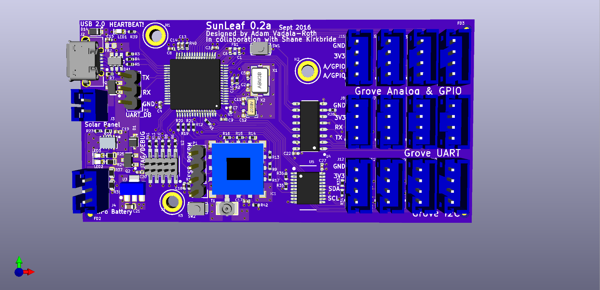
Electrical things where not the only part of the work done on SunLeaf 0.2a. 3D models were added to more components for proper 3D rendering of the board. This is important for designing a new 3D printed case for the 0.2a revision. KiCAD does a great job at rendering and showing the board, its super smooth and very fast. Here are some pictures of the render:

Top:

Bottom:

With that there are only a few more tweaks to do before fab, mostly adding test points. For testing this board the plan is to make two layer board with pogo pins tapping the connectors from the bottom. This method should eliminated the need for most test points, either that way ore the board will sit upside down in the test jig. More on that stuff in the next update!!
 AVR
AVR
Discussions
Become a Hackaday.io Member
Create an account to leave a comment. Already have an account? Log In.