 Alex Hunt
Since receiving my first PCBs there has been a flurry of activity. Naturally, the first thing I did was to solder one up:

Having never used SMD components before I was pretty pleased with the results. For the moment I am attaching the Piezo sensor with crocodile clips to the top two holes. The wires on them are quite delicate and I was concerned they would break. After an anxious few minutes uploading the code, I am delighted to report that it works!
Light-headed with success I decided to complete the PCB design for the bracelet part. Having learnt a lot from my first experience, I was feeling slightly more ambitious and this is what I came up with: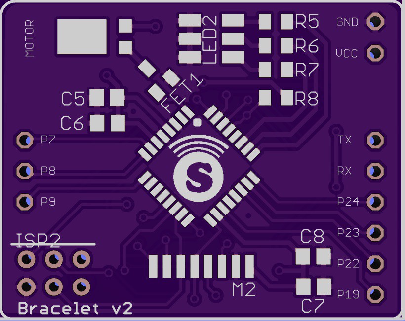
I decided to break out the RX and TX pins to help with testing and also some other unused pins as I have a vague plan to add a button in future for muting the bracelet.
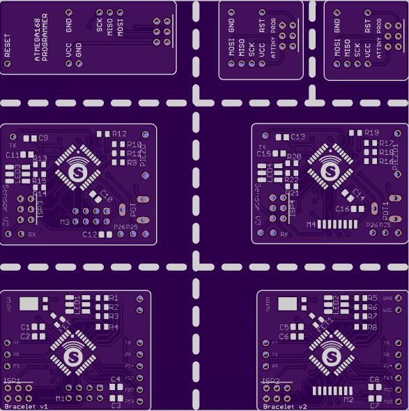
By this point I was overcome by confidence and decided to update the sensor board as well. I have swapped the large NRF24L01 for one of the mini-boards, added an LED (again, future plans for this) and broke out a couple of pins. Finally I decided to panelise my designs and also add in a couple of extra boards to make programming the DIP ATMEGAs and TINYs easier.
Now it's off to the folk at smart-prototyping to work their magic. I used Maker Studio for the first round of boards and was delighted with the results. However, smart-prototyping offer slightly cheaper express delivery and so I'm going to give them a shot.
So what's left to do? A few things spring immediately to mind:
- Optimise code for power consumption (the sensor eats through a watch battery in about 2 hours with the current simple code);
- Add a wifi bridge to the network of sensors to allow smartphone notifications;
- Design some sort of case for the bracelet / sensor boards.
Other suggestions are always welcome.
Discussions
Become a Hackaday.io Member
Create an account to leave a comment. Already have an account? Log In.