 bosko
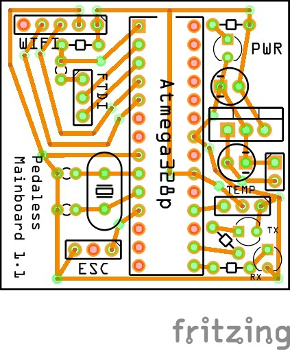
boskoAfter first prototype was tested, and was pass all tests like hardware and software i was working on new PCB of Mainboard, this version is still one layer PCB because easy for me it was to make it one layer. In pictures you can see PCB design and after soldered. Also in TOP side of PCB i add silk layer.
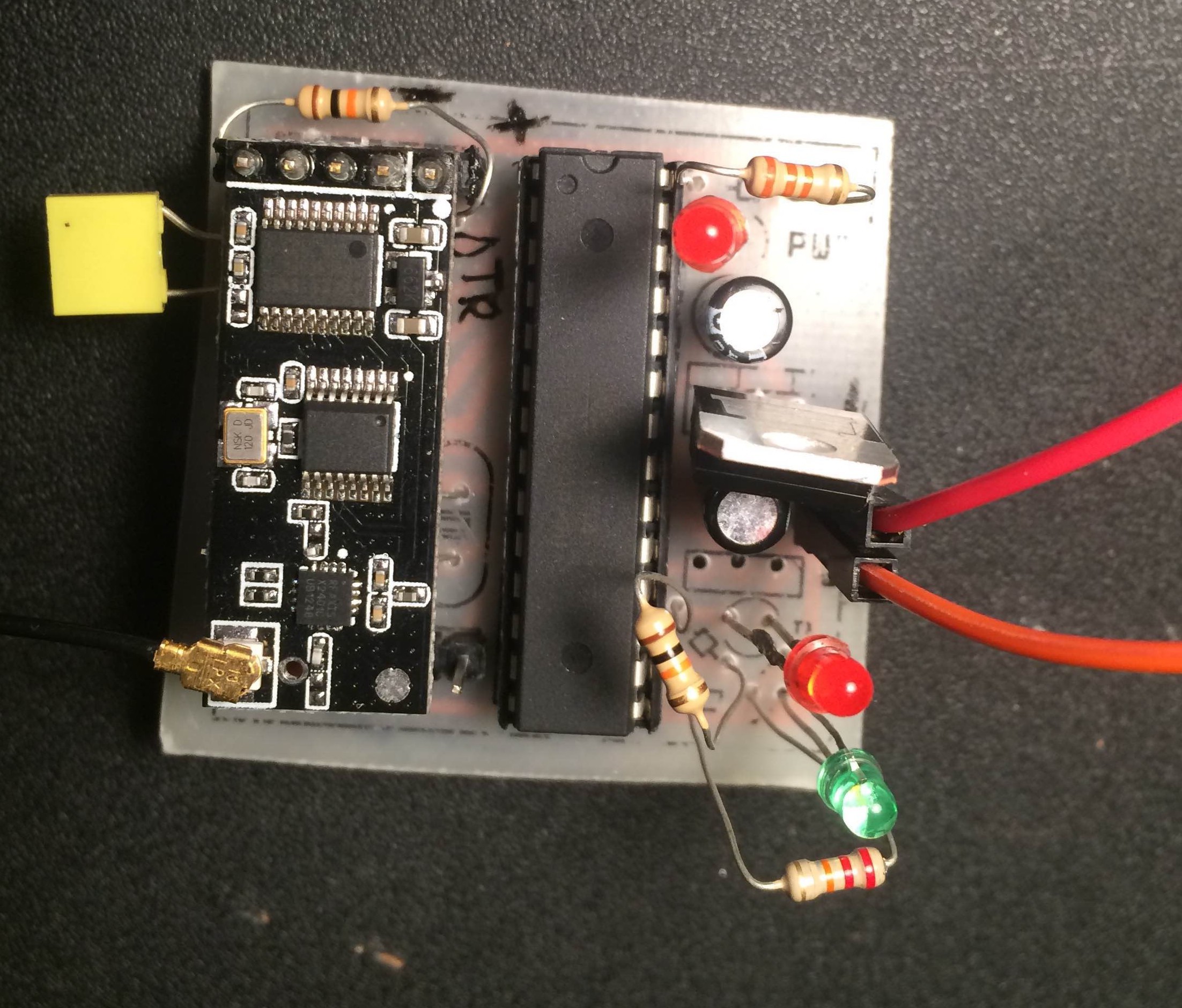
In next picutre you can see soldered and tested, all works was fine.
Discussions
Become a Hackaday.io Member
Create an account to leave a comment. Already have an account? Log In.