How will the fast speed be accomplished ?
Relays are slow, and to get acceptable performance, many measures must be taken.
Architecture:
- Microcode will not be used
- Harvard architecture, so fetch and execute will be in parallel
- Have enough registers so we're not loading and storing all the time
- Have a good instruction set
- Some special instructions tailored to the algorithms that are used
Technology:
- Design in such a way that for executing an instruction a very low number of consecutive switching relays is needed. At this moment, there are only four consecutive switching relays for an instruction.
- Use small relays, these can be fast (datasheets show 2 msec switching time). Using small relays means they take less space on a pcb, so not much pcb area will be needed.
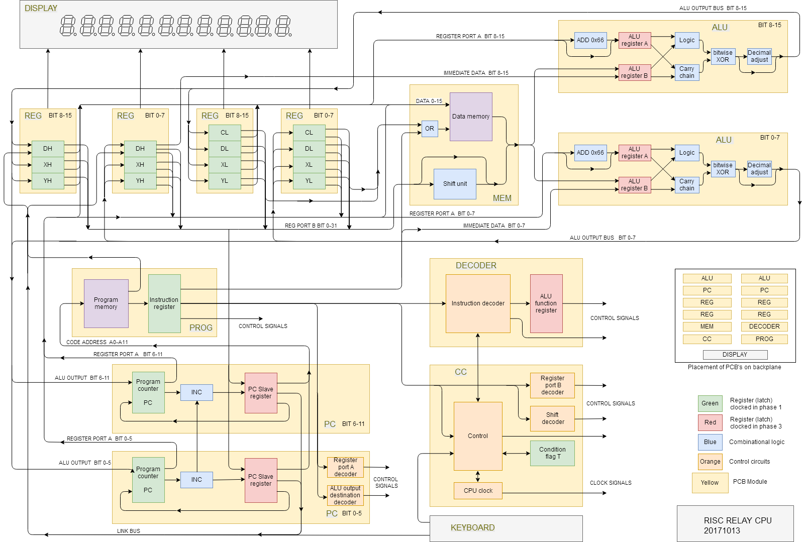
The design is shown in the following block diagram (click on it for a larger version):

The block diagram also shows which functions the twelve PCB's and the backplane contain.
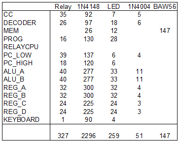
Now that all schematics and also all pcb's are designed, I can give a quite accurate listing of the number of main components:

SIMULATOR
There is an online browser-based Assembler and Simulator that simulates the calculator application (or any other application that you could make). Just press "Assemble" and then "RUN", and start making calculations on the calculator keyboard that is on the screen. (After each button click, have some patience until the script halts and the number (hopefully) appears.) The calculator program does not give messages yet for overflow, or out-of-range input (including zero divide). Trigonometric functions don't work yet, all others do.
ARCHITECTURE DETAILS
The architecture is explained in the architecture document (see Files section). Highlights are:
- All instruction, register, word and memory sizes are 16 bit.
- Most instructions operate in a single cycle.
- There are eight 16-bit registers, one of them is the PC.
- Six registers can be paired to form three 32-bit registers (like the H and L registers in the 8080 / Z80 ). Many instructions have a 32-bit variant that operates on register pairs (using 2 cycles but single instruction word).
- It is a 2-operand design, 1 operand is a register and the other one can be register, memory, or immediate. If the immediate is only 8 bits (7bits + sign), it is included in the 16-bit opcode and the instruction executes in a single cycle.
- Memory addressing always has a small displacement within the instruction opcode, facilitating addressing of variables in a stack frame, or addressing of structure members. Instructions that use this need only a single cycle.
- The ALU has also decimal instructions (in addition to the normal binary instructions), to support the calculator functions.
- There is a special instruction to support (decimal) multiplication.
- The ALU has special instructions to convert the 4 nibbles in a register to bits that control a 7-segment display.
The architecture is independent from the technology, so it could also be used for a TTL or FPGA design. It can be upgraded to a full 32-bit design. Actually, since there are 32-bit register pairs, it would be easy to support a 32-bit address bus.
Use of the architecture is free for non-commercial use :), but I would like to get a mail when you are going to use it.
PROGRESS
What has to be done:
- Have an architecture.
- Have a schematic.
- Have a simulation. The 4-bit boards have been low-level simulated in Logisim. I do not have a good logisim model for a relay, so the simulation might not catch all problems. Many instructions have also been simulated.
- Built an assembler and simulator. Simulating the application before the design is finished gives a chance to optimize the CPU for the application. Available HERE.
- PCB design
- PCB ordering
- Build an 8-bit version (this does not need all PCBs)
- Build a programmer for burning the flash memories
- Have a test strategy, and test.
- Find the causes of problems, and correct them
- Build the full 16-bit version
- Debug the full version (now, january 2019)