Still working on the schematics. A lot of little details must be handled:
- splitting clock signals, in order not to overstress relay contacts
- program counter is 12 bits, add 4 bits and a selector knob to switch between several programs in two 64K x 8 flash chips
- how to get the program in flash... provide connector for dedicated AVR-based programmer with RS232/USB connection to PC
- The dedicated programmer should have buttons for manually composing an instruction and execute it
- The clock signals must be made. Clock must be started and stopped.
- User input buttons must be handled
- The remaining pcb's (except main pcb) will be made smaller than the first ones, now I discovered that 10 x 10 cm boards are a lot cheaper than bigger ones (at certain pcb makers).
- How to distribute the remaining circuits over several pcb's, and how to allocate signals on the 96 pin connectors
The last point has great influence on the routing of the main board. So, the main board is routed first. The connector allocation can still be changed if needed (except for the existing register and ALU pcbs). Here is the current status:
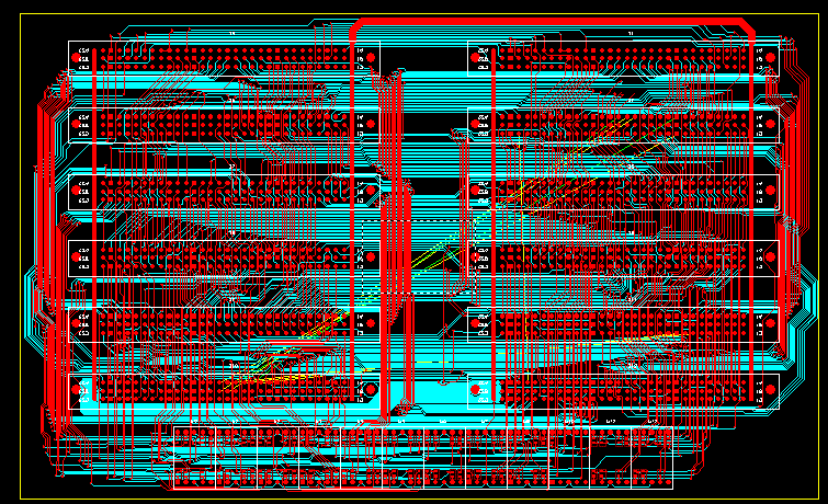
There are two rows of 6 connectors. At the front, there are 12 displays. The yellow signals must still be routed. But there will be more to do, since the schematics are not complete yet. This will keep me busy for a while...
The ALU has now all 8 bits built, and is working after solving a few soldering issues.
Discussions
Become a Hackaday.io Member
Create an account to leave a comment. Already have an account? Log In.