Introduction
Bipolar is not only a disorder but also a requirement for power supply for some devices. While most electronics is OK with a simple plus and minus, some will also require a mid-point, often called ground. It does not have to be connected to a real Earth ground and sometimes that is not even possible (think satellites).
The problem is that many laboratory power supplies do not have this midpoint, though they frequently offer ground connection. But that can only be tied to plus or minus, no real midpoint is typically available on them. That's where a virtual ground comes to save the day. Virtual ground, also called "rail-splitter", is a device that creates a midpoint, whose voltage is (plus + minus)/2 and is capable of both sinking and sourcing current. There are two basic approaches to get virtual ground: Either from a switching regulator or from a linear one. The former is more efficient and the latter is easier to build and offers less noise, albeit at the cost of wasting half the power.
For projects that do not require high power, a linear virtual ground is
appropriate. I am presenting a circuit and a board that I use
personally. It is a third iteration of my original design using a power
op-amp and a simple resistor divider.
The construction
The unipolar power enters through an universal screw clamp terminal (CON1), the positive rail passes through a 3A resettable fuse F1 (PTC). Voltage spikes are quelled by a bipolar (can be unipolar too) transient suppressor diode D1. The positive rail then passes through reversed P-FET transistor Q1 that protects the circuit from reverse polarity. A suitable part for Q1 would be Vishay SUD50P06-15, a cheaper alternative Infineon SPD18P06P G might work too. Gate voltage is regulated by Zener diode D2 and current-limiting resistor R1. The gate voltage must stay below what is in the datasheet (typically 20 V) so choose the Zener voltage few volts below the FET's maximum (see my earlier blogpost about reverse polarity protection). The rail then continues from Q1 to three bypass capacitors for the main op-amp. C1 is an aluminium electrolytic capacitor, C2 a large ceramic capacitor and C4 is not shown because it is supposed to be soldered directly between pin 4 and 5 of the op-amp. Use 0603 package and 100nF/100V with X7R dielectric.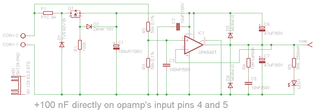
The voltage from the input terminals is divided by two thin-film precision resistors. Use at least 56k because if the polarity is reversed, some current will go through these resistors and the ESD diodes of the op-amp. Its value should be small (like 1 mA). The output of the resistor divider is one half of the input voltage, this, after being buffered, will be the virtual ground voltage. The output from this resistor divider is stabilized using capacitor C3.
The heart of the virtual ground is OPA548 – a high-end power operational amplifier from Texas Instruments (IC1). It is capable of continuously outputting 3 A. Its input voltage must be between 8 and 60 V so the virtual ground will be 4 to 30 V above the negative power supply. Since this is a linear virtual ground, the op-amp must be attached to a heatsink. With Fischer Elektronik SK 129 63,5 STS, the thermal resistance of the system should be around 5 K/W so the virtual ground will be capable of dissipating approximately 20 W. But I haven't tested it at this power dissipation.
The output of IC1 is buffered by two identical aluminium electrolytic capacitors – C6 and C7 – before entering the output banana receptacle. A snubber circuit aimed against oscillations is formed from a series combination of resistor R4 and capacitor C5. Two reverse-biased silicon diodes (D3, D4) protect the output of the IC1 against voltage spikes that often occur from inductive loads. A suitable diodes are MUR410 from ON Semiconductor. Fast recovery is a key factor here.
Finally, there is a green LED (LED1) with series resistor R5 indicating that the output is on.
How to calculate...
Read more »
 Szoftveres
 Hamza Deniz Yılmaz
 w_k_fay
 Sagar 001