 Kuldeep Singh Dhaka
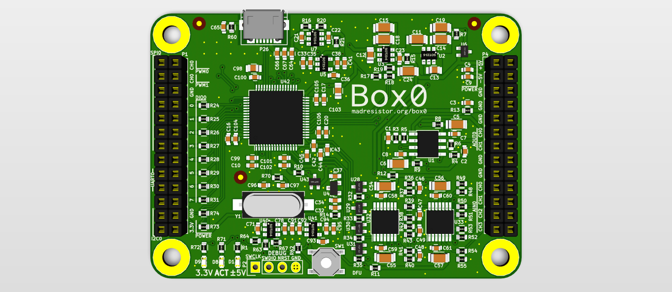
3D Top - with components (computer generated)
3D Top - without components (computer generated)
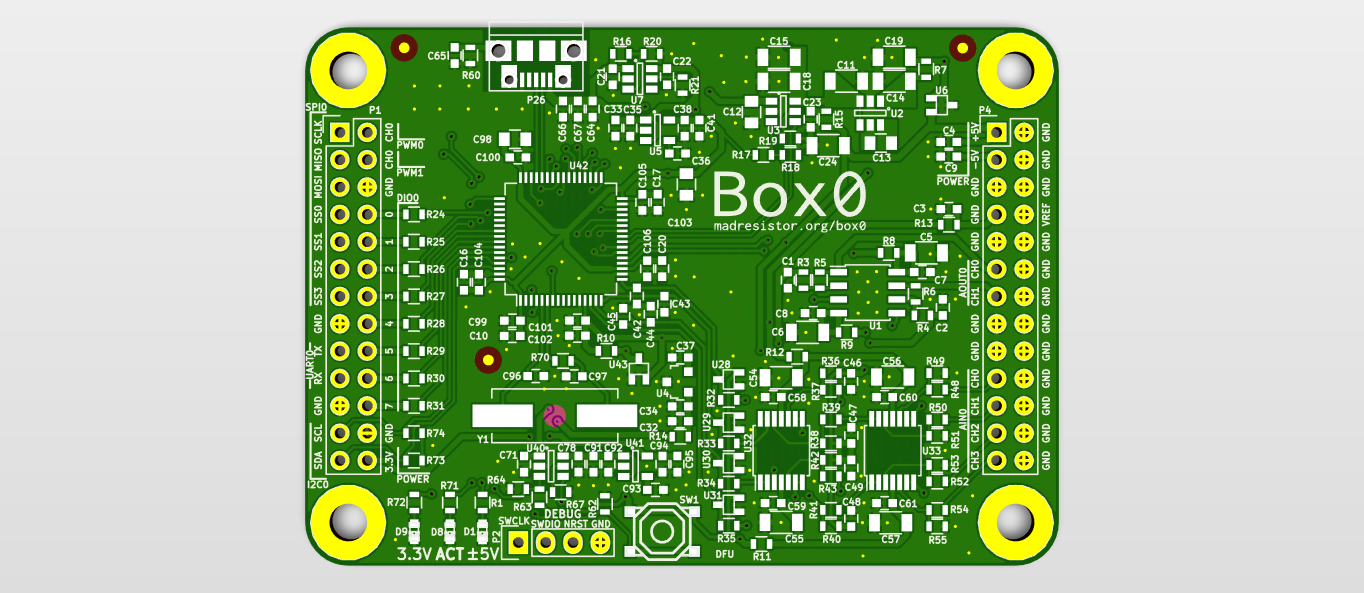
 3D Back - with components (computer generated)
Filled Top
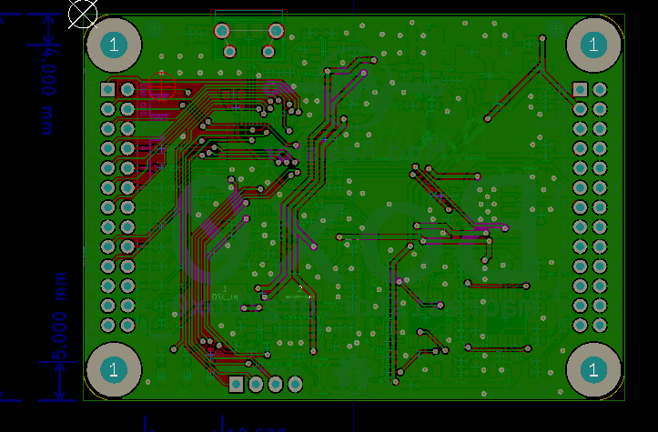
Filled Back
Unfilled Top
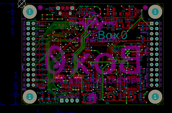
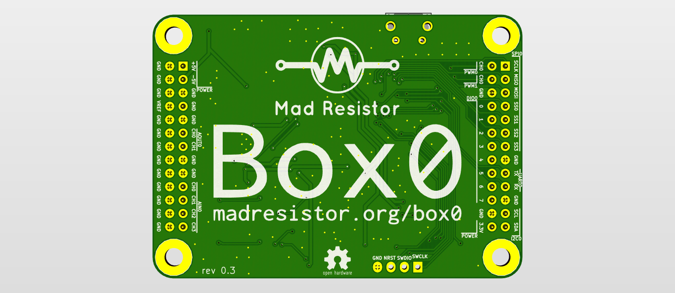
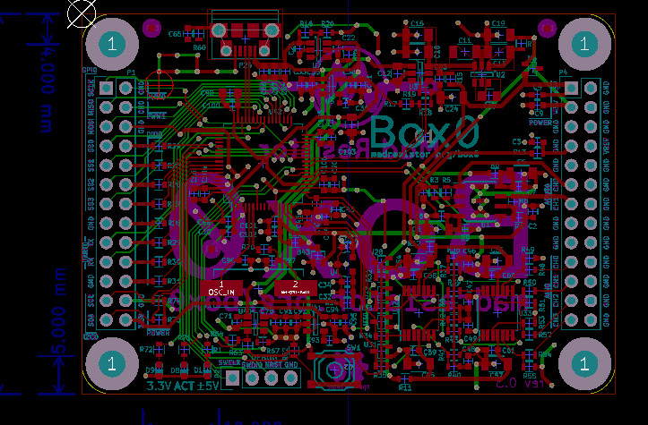
Unfilled Back
You get the KiCad files from git repo here.
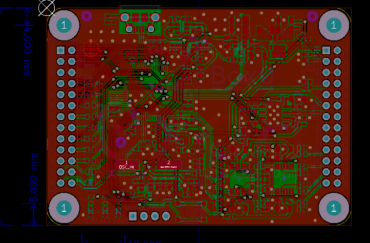
2 Layer design, while designing, it was a goose chase to get the right position and connection!
In the charge pump (-5V from +5V) block [and other power management block]:
Special care have been taken to reduce the loop (high current path). by using Via and minimal cut in ground plain.
To make the connector even more stronger, we placed copper under it.
So that the connector can get even more strength from the solder.
Discussions
Become a Hackaday.io Member
Create an account to leave a comment. Already have an account? Log In.