 Shayna
Shayna : PCB Artwork Hack Chat starting soon, everybody!
Shayna : Post your questions in the discussion on this page :) https://hackaday.io/event/112119-pcb-artwork-and-photo-conversions
Just was looking at some of my really old PCB art... :-D
http://www.retrotronics.info/modules/news/article.php?storyid=14&lang=english

RETROTRONICS - FDC 3.2 - Floppy disc controller for Pravetz 8D - New in the collection - NEWS
FDC 3.2 - Floppy disc controller for Pravetz 8D Read this on Retrotronics
Hey
Shayna : Hey @Andrew Sowa !
Shayna : Thanks for joining us for this Hack Chat today
Shayna : We'll get started in around 10 mins or so
Wahoo, I'm looking forward to this one!
Shayna : Before we get rolling, would you like to tell us a little about yourself @Andrew Sowa ?
I'm a electrical engineer from Chicago and for my day job I make LED light fixtures. I am a contributor to the Supply Frame Hardware blog and
got start with PCB art stuff by making the Benchoff Nickel after a long night on Kicad layout for a crowdfunding project I was working on
Since then I have evolved that into my signature style for lack of a better phrase of turning photos into pcbs.
Shayna : awesome!
Shayna : Mind if we get started on the questions?
I'm ready
Shayna : Please also feel free to share any images/projects you'd like folks to take a look at, too

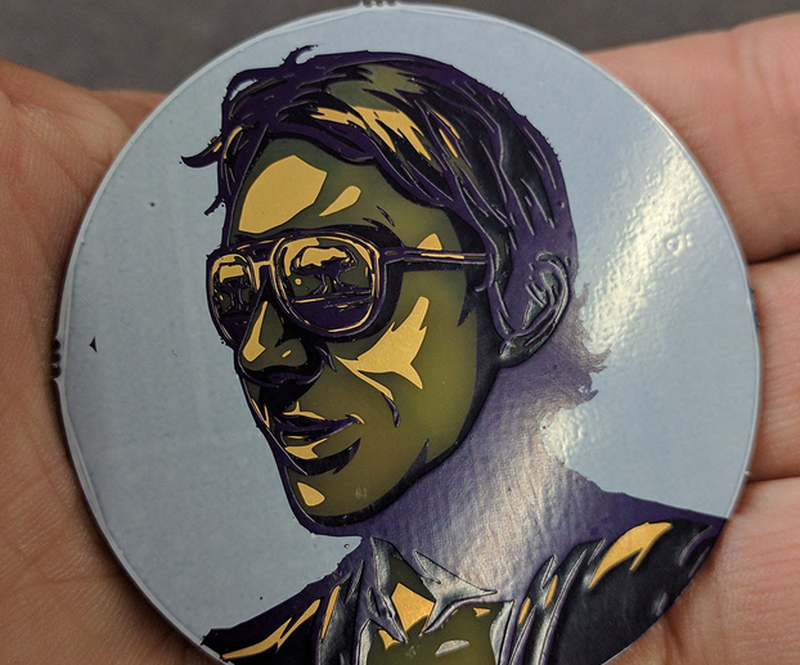
Shayna : I think I know that person :)
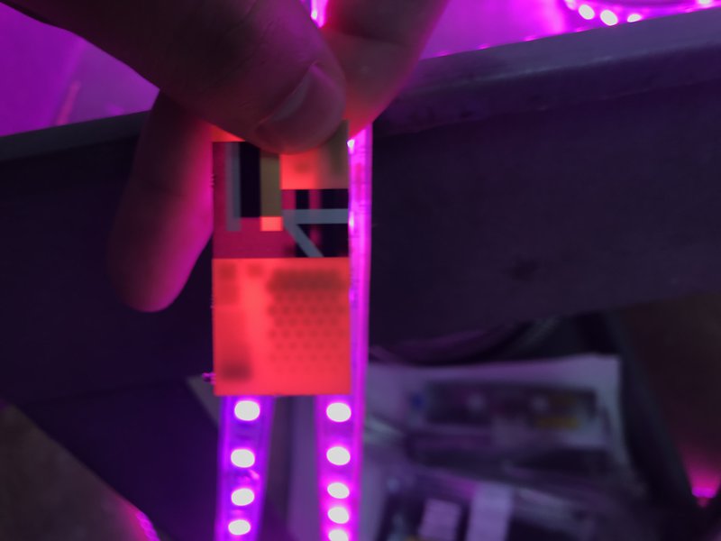
This is my latest project. It was requested that the hair needs to be pink so I have been working with halftones to make the contrast while also back lighting the bare FR4
where does the pink come from?
Shayna : Very cool
Shayna : Alright, first up from @zakqwy : "I do a good bit of Inkscape --> KiCad graphics work and am by and large happy with the process. However, a lot of my custom graphics also function as electrical elements, usually ground planes or touch sensors. Any thoughts on making custom footprints that KiCad actually recognizes as such for routing and fill purposes? Right now wiring graphic bits up to a circuit is a process that can't take advantage of KiCad's excellent on-the-fly DRC bits, making the technique prone to errors."
I just figured out how to do this while still keeping the DRC working this morning
ah awesome! share your secrets!
i would love push 'n shove to route around my copper graphics
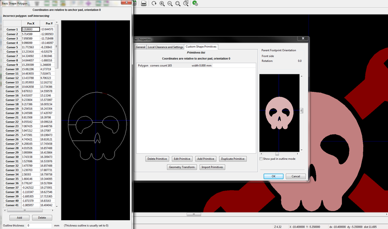
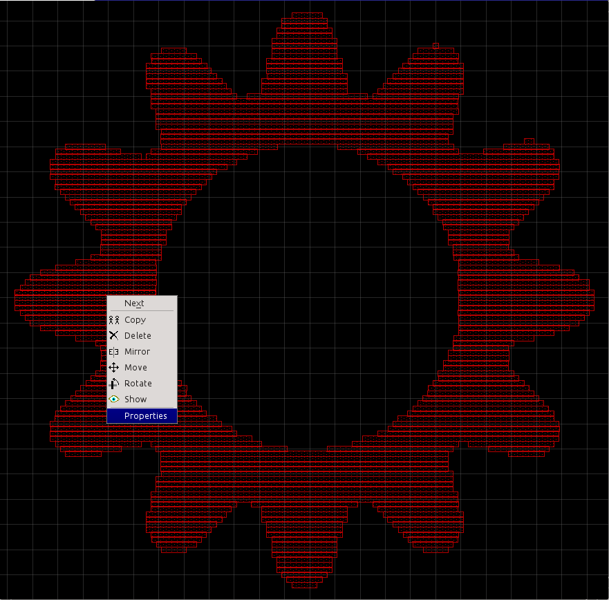
In Kicad 4.0 you could only do specific shapes for footprints so any polygon gets put in but not processed properly from a DRC perspective. There is also an isssue where the edge cuts also don't get caught with DRC
i like when you can integrate your artwork witht he electrical connections
with 5.0 the edge cut thing is fixed but they also added arbitrary shapes for footprints
can i still import 'em via bitmap2component from an *.svg file (or elsewhere)? or do i have to make the footprint itself in kicad?
You can use the bitmap converter to get all the points you need to put into the text file and use this new formatting to get it to process correctly. This is a little hard to explain in text but I'll try my best
What's the edge cut thing?
https://github.com/Junes-PhD/kicad_arbitrary_pad_example

Junes-PhD/kicad_arbitrary_pad_example
kicad_arbitrary_pad_example - Using bitmap convert to create complex shaped footprints Read this on GitHub
there is a distorion pedal design in which a guy used the map of old east/west berlin and used the wall and subway lines as actual traces and even got so far that he used actuall border crossings for places to put diodes etc
and iirc the airports where signal in and out
http://oree.storijapan.net/praxis/distortion/

Ore.e Ref. - Distortion Sounds of Labor for share Read this on Storijapan
Shayna : ha!
good to know it's supported in kicad 5 -- i haven't taken the plunge yet but will investigate. thanks!
Andrew Sowa : I'll get to edge cuts in a sec. There is a new panel when you make a custom footprint and that lets you manual add points. The inject button doesn't work but it's much easier to manage the text file anyways

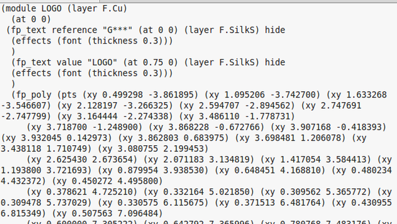
This the new format. Basically you need to replace all those XY points with what shape you want. To get those points you can use the bitmap tool or an svg converter.
https://github.com/mtl/svg2mod

mtl/svg2mod
svg2mod - Convert Inkscape SVG drawings to KiCad footprint modules Read this on GitHub
Andrew Sowa : https://github.com/badgeek/svg2shenzhen-next

badgeek/svg2shenzhen-next
svg2shenzhen-next - Inkscape extension for exporting drawing into Kicad PCB Read this on GitHub
ah cool. yeah, it looks like i could use a standard kicad_mod file and replace "fp_poly" with "gr_poly"
It's not super easy to transfer but easy enough and likely scriptable. Just figured it out so haven't optimized yet
sweet. i'll give it a whirl. thanks @Andrew Sowa !
Those two links are svg to kicad footprint converters. I haven't tried the second one yet but I used the first one for the OSHWA logos
^ ah hadn't found svg2shenzhen. Tried converting SVG to kicad in inkscape this week for the first time and... oof
I have broke these converters before so my process is a little different right now.
Shayna : When you're ready -- next question is from @ðeshipu : "A lot of the PCB art discussion seems to focus on importing images into programs that clearly are not designed to do this kind of thing. Why not just use Fritzing and be done with it in 3 minutes?"
I don't use Fritzing because I never learned it and I also want to integrate graphics into working pcbs
It's likely a perfectly good solution but I just haven't tried it yet. I also know Eagle has some features and adding more. Nick Poole just posted a program that's suppose to help with eagle files that I haven't tried yet
Jumping back to the edge cuts thing. Before kicad wouldn't be aware of where your board outline was so you could run a trace into mid-air. That is now fixed and I no longer have to add dummy wires to keep me from getting to close to the edge.
even with imported *.dwg edge cuts?
What about BoldPort's PCBmodE?
It should work with imported dwgs but I haven't tried that yet. I often make outline in fusion 360 because it has better snapping and import. The only issue is that you can get tiny gaps that you have to fill between curves
I tried to get PCBmodE but couldn't get it to work on my windows machine. Haven't invested the time to learn it yet but BoldPort does amazing work with it and I would say it's better than the stuff I do lol
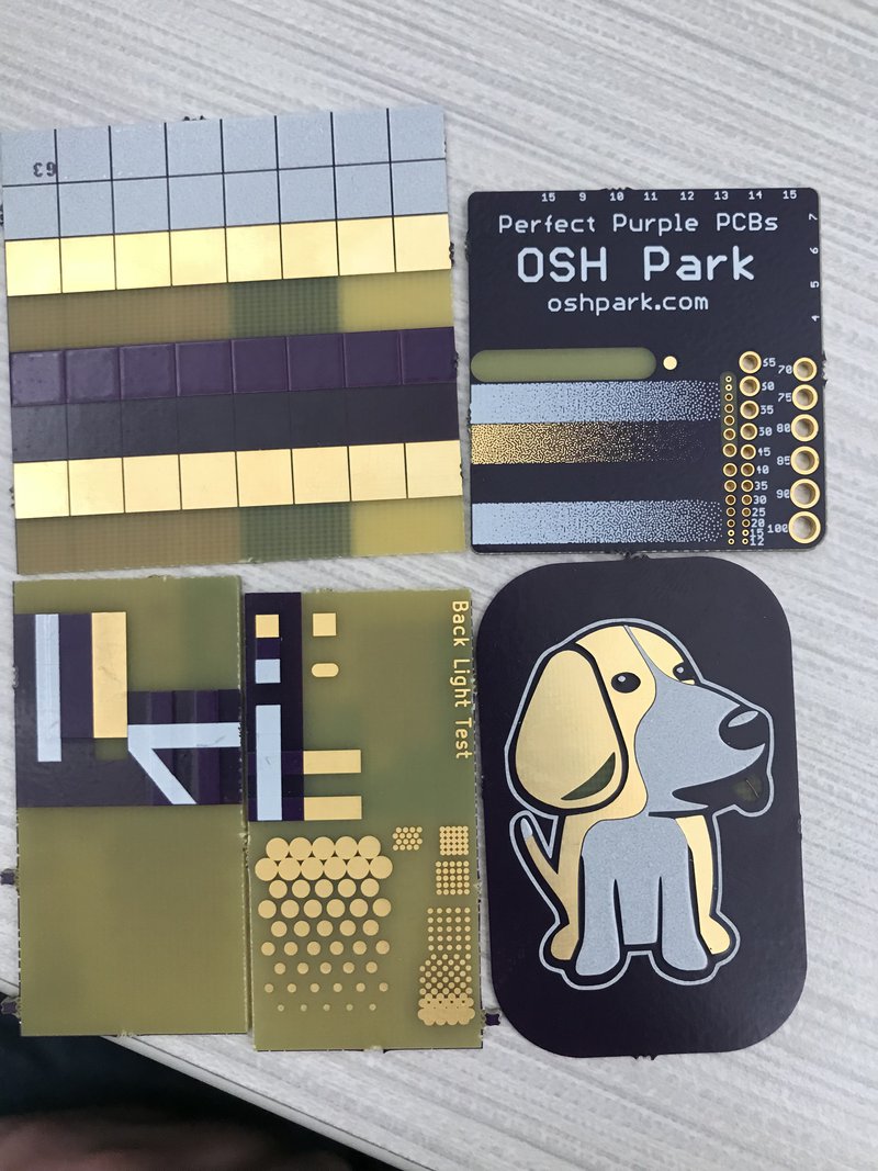
Can I ask about anyone experience with osh and raster images? I want to push to the limit silk screen.What is max DPI for it? Lokking at my old order I assume 1000DPI is achievable due to photorestist limits:

m1
Image m1 hosted in imgbb.com Read this on imgbb.com
The render on the well can only do I believe 400 dpi, rush is 400 or 500 dpi, and standard two week is 1000dpi
@Robert Mateja I usually do raster stuff at 500 dpi, keeping in mind minimum line weights
Yes, for our standard service, we use LPI silkscreen which is 1,000 DPI
dang standard > rush in terms of resolution?
TIL
the process takes too long for quicker turn, so our "Super Swift" uses inkjet which is 500 DPI.
we list 500 DPI in our spec as a result
http://docs.oshpark.com/troubleshooting/import-bmp/
OSH Park Docs ~ Troubleshooting ~ Including bitmap logos on silkscreen
Our process is not properly equipped to handle features of that size, so we cannot guarantee that they'll be printed correctly on the final board. The maximum DPI we can correctly process is 500 DPI, corresponding to pixels of 2 mil or larger.
for anyone that wants to make sure they get 1,000 DPI with LPI, just email support@oshpark.com and we can make sure of that
Ok, much thanks for confirmation!
Shayna : Next up is from @Eric : "I'd like to learn how in KiCAD to invert the silkscreen so that my component references mask the silkscreen. I have my PCB ready and am just about to try applying more of an artistic flare to the functional pieces I have now. Also hoping to learn about production issues for example are there any issues applying silkscreen to bare copper? What else should I know?"
I am a little confused about inversion I believe they mean want the text to be the color of the solder mask? I is bad to put silkscreen on copper but I believe most fabs will clean that up for you. @oshpark could probably better answer that
I don't know of an easy way on inverted text. My quick though is to treat it as an image but that is a pain to change all the time. There maybe a plugin for that somewhere but I don't know of one.
https://www.youtube.com/watch?v=2JZ428Gxnrc&t=2s&ab_channel=AndrewSowa
awesome!
Shayna : awwww
this is generally my workflow. which may help some people better understand what I am referencing
Shayna : very cool
Prepping for this I realized that I need to make more video better it is hard to explain some of this with static images
Shayna : Workflow question from @ðeshipu : "Why not reverse the workflow? Do the routing first in your favorite CAD program, export the gerbers, and then edit them in a graphics program to add the artwork? Wouldn't that give us more control over the result? Are there graphics programs that can read gerber files? Would it be hard to create an import/export plugin for Inkscape or GIMP?"
I'm more of a hardware person so I am not the person to ask to make a plugin so I don't know the difficulty. I know gerber has a specific format that is a semi-loose standard. It should be theoretical possible but I haven't had the need to work this way.
If in this board, I wanted to include a component with text (being an area not screened in white) Can I easily mask that? Was this area created as a fill but on the silkscreen layer?
plus it's nice to have the DRC which makes native formats benefitial
The way that fill is made right now there is not an way to do it in kicad. There is a way to generate fill zone with odd shapes but I don't think that will work will silk screen layer.
https://www.youtube.com/watch?v=H-Lc91iaH6w&ab_channel=ContextualElectronics
see that video until I actually make my own
Thanks, I've watched that one. Shout out to Chris for some awesome videos!
Thanks to you too of course for being here today. truly appreciate the time and effort.
Shayna : So, we're soon coming up on the last bit of the questions in the comments: https://hackaday.io/event/112119-pcb-artwork-and-photo-conversions
Shayna : If you want to add more to the list before then, please feel free to do so in the meantime. Otherwise, we can open up the discussion after the last question for as long as @Andrew Sowa is able to hang out :)
Shayna : @ðeshipu asks: "Do you know of any PCB pixel art?"
I am not sure if they mean 8-bit style stuff or halftones
my favorite half tone one is the flower Drew often shares which I don't have a picture on hand.
nice !
https://www.wired.com/images_blogs/threatlevel/2010/07/defcon_ninja_eecue_003_badge_back.jpg
halftone example is in the topright. That is not my board but a good example of the grey scale look you can get. I am actually having trouble generating that file well in Kicad and may have to try some other programs.
Let me find the flower
:-) better than my old attempts :
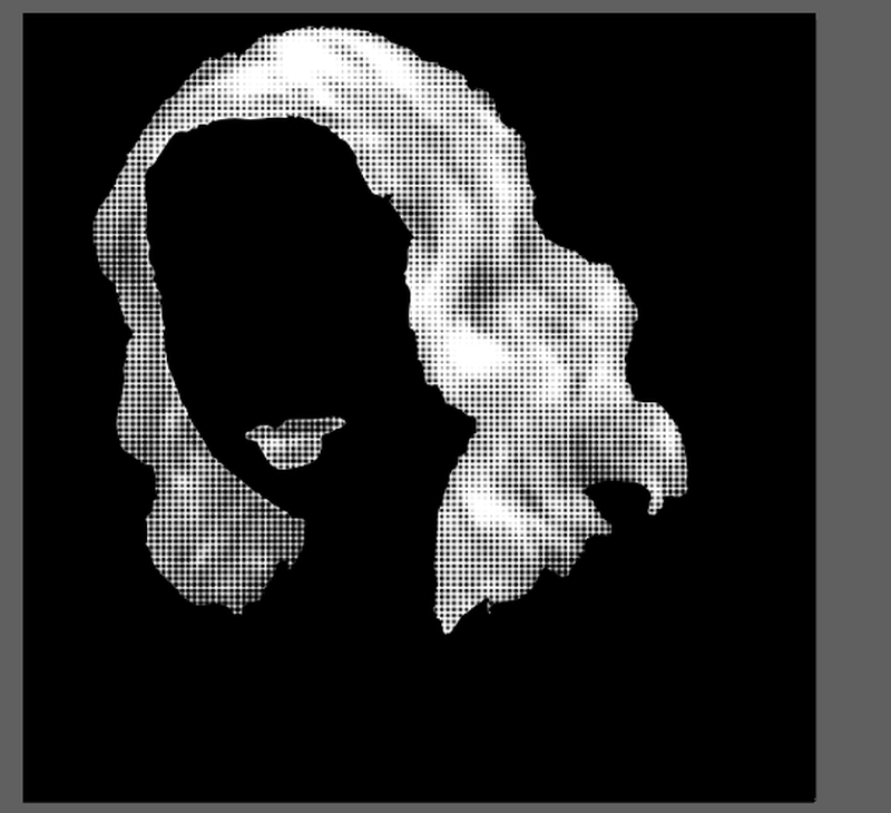
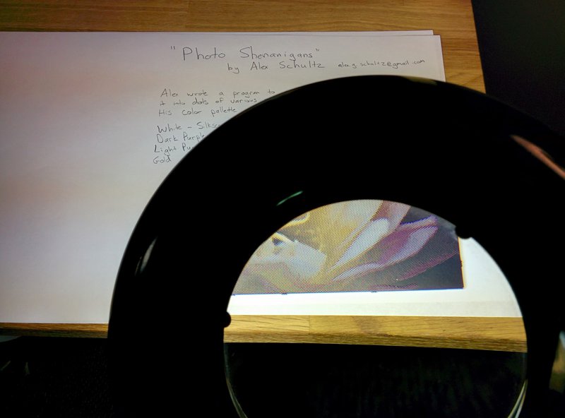
The lady ada project is going to rely on halftones to create the hair shape with back lighting but bitmap import hates all those small circles. Illustrator even complains when I vectorize it.
http://blog.oshpark.com/2016/09/30/recap-of-pdx-maker-week-open-house/

Recap of PDX Maker Week open house
Thanks to everyone that visited us during our PDX Maker Week open house! We always enjoy meeting our customers and showing projects built by our team. Here's more information on the Drawdio for those that got our PCB giveaway: Adafruit Tutorial Parts List Laen displayed his new Dazzle project with Neopixel matrix controlled by a Teensy:...

https://plus.google.com/photos/100779964808096572793/album/6333017586389944753/6333018299769760674

Album - Google+ Read this on Google
Shayna : beautiful
now that's sexy right there
wow, @oshpark any chance of dimensions of this piece?
@Robert Mateja looking it up... it was about 3 inch by 4 inch
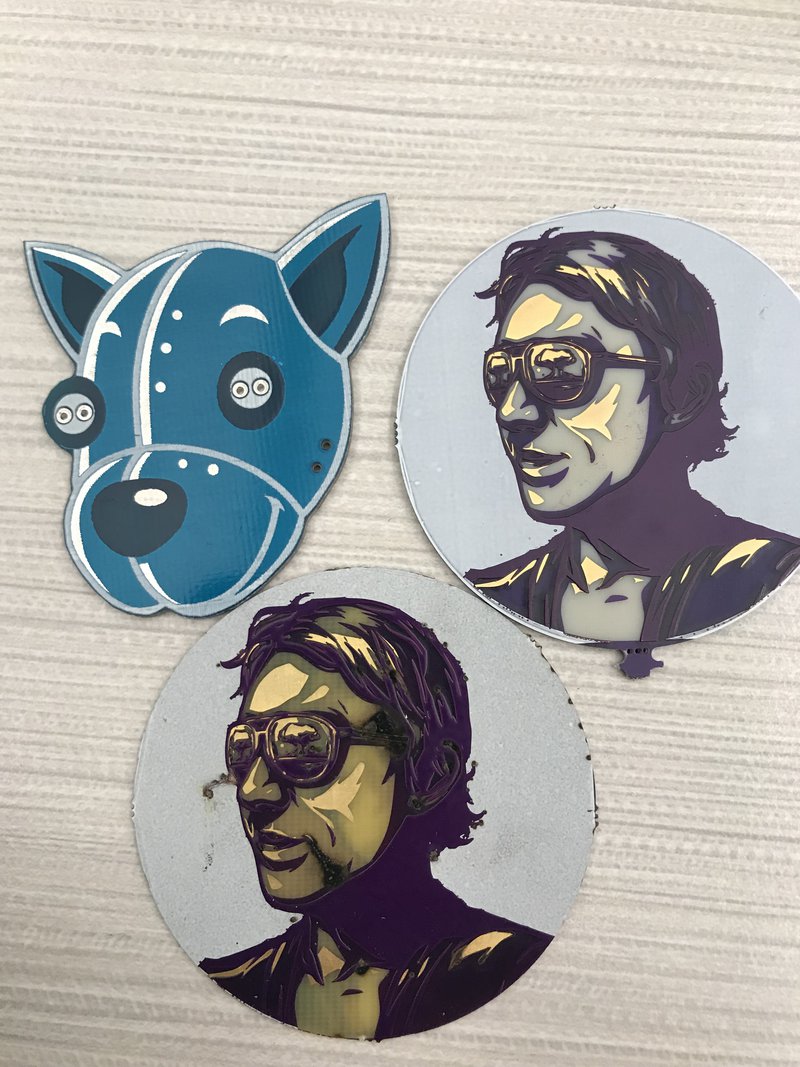
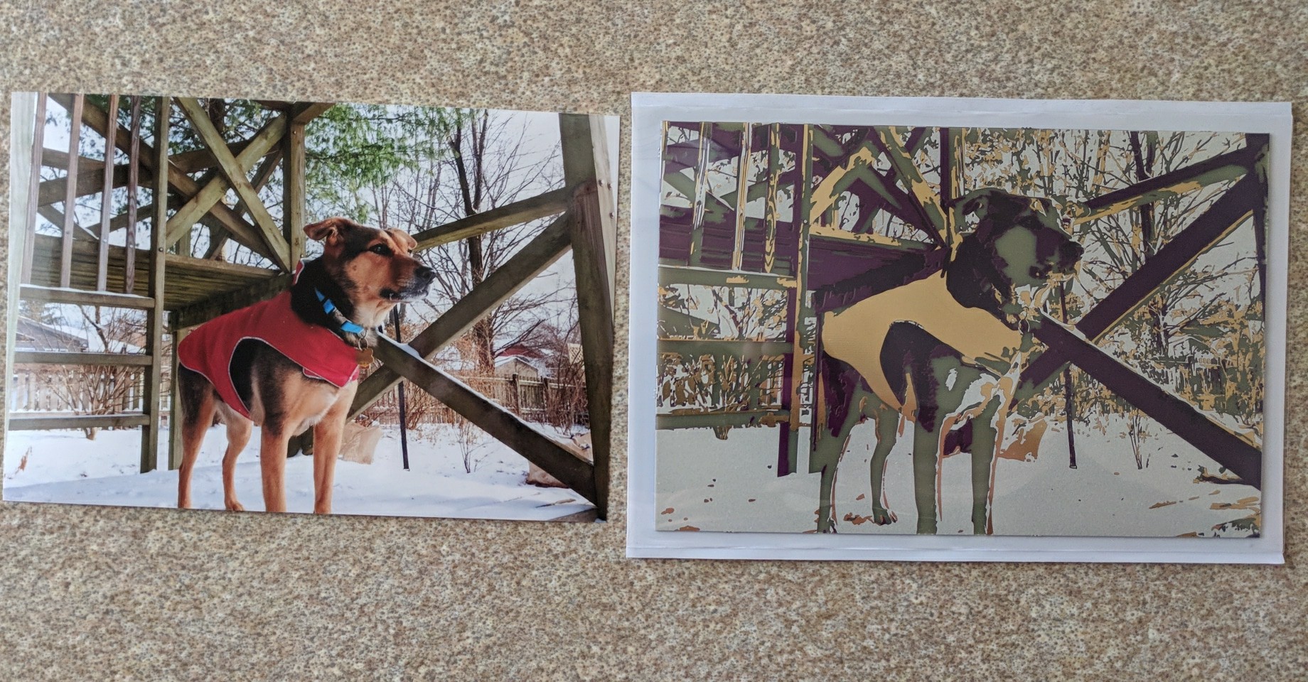
The basis for most of my stuff is image trace in inkscape or illustrator. It does most of the hard work then I need to go in and create contrast. In this one I trace it to 16 colors and manual change things until i got back to 6
https://oshpark.com/projects/IO45CK3f/
OSH Park ~ Read this on Oshpark
Shayna : Thank you so much @Andrew Sowa !
Shayna : That's it for the questions on the comment page, but I hope you can stick around with us for a little longer
Shayna : this is a fun topic :)
I love these works !
Thank you Andrew!
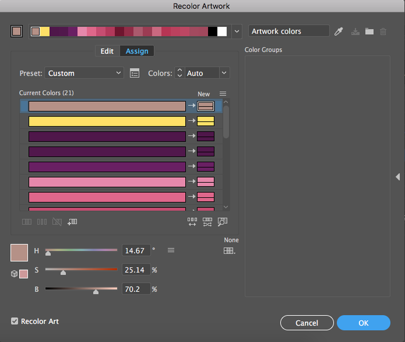
this recolor artwork tools is the main reason I use illustrator but all my early stuff was done in inkscape.
mfw i open the ss then try to click the cancel button
The best other tip I have that I mention briefly is that complex board outlines are usually better drawn in other programs.
zakqwy : One question re: outlines -- I make most of mine in Inkscape and it's a bit annoying to have to 'segmentize' bezier curves. Is that still required in KiCad 5?
yes
ah well. Still a great program.
eagle is working on it but dev said is not top priority
This one required arc nears arcs and generally annoying to make in Kicad , but with Fusion for example its easily done to specific parameters if you need an exact shape or parametric shape.
This is drifting in practical things but that could also be a sketch from a mechical engineer making the enclosure.
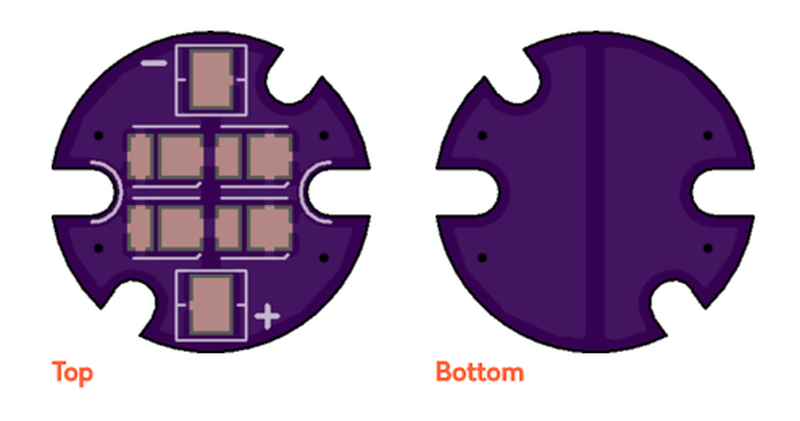
The last thing I have from my notes is the different colors between two and four layer boards. These use different fiberglass materials and have a different color
Top right is a four layer and bottom center is two layer with same design files
Do you ever use interior layers to add shading?
The bottom one is beat up because we arced 10KV into during super conference
yes, our 4 layer is Isola FR408 which is white.
versus the normal tan color of FR-4 in 2 layer boards
I have not yet. I was working on making Carl Sagans golden record but I never finished that. I wanted to make gaps in the copper/enig to look like the track lines and add the center art in middle layers
I made the map part. Looks good in ENIG.
There will be a 4 layer board at super conference but that more of a joke piece and a secret for now
just joined so sorry if you already mentioned - how did you achieve the layered hair effect on Benchoff? is that just mask with/without copper?
mask on bare FR4 vs mask on copper. The copper lightens it up
gotcha, figured. thanks! and was great grabbing a beer with you at con :)
http://andrewsowa.com/blog/2017/3/19/creating-the-benchoff-nickel

Creating the Benchoff Nickel
Idea I thought of making the Benchoff nickel after I saw Brian's Hackaday,io profile. He has a hi-res image of the center a Benchoff Buck which is well suited to being converted to a PCB. There is only a few colors and they have sharp edges. Bitmap2Component in Ki
sweet ty
I have been busy for the last 2-3 years with various crowdfunding campaigns so I never had time to document all this as much as I want too so since I'm pretty sure I'm done with crowdfunding I have more time to dump all this information
I guess i should mention I will be talking about this at crowd supply's teardown next month.
Yeah!
looking forward to it!
@zakqwy will you be at Teardown in Portland?
https://www.crowdsupply.com/teardown/portland-2018

Teardown: Portland 2018
A party for hacking, discovering, and sharing hardware
yah, found a cheap flight!
awesome!!
I post most often to twitter @junesphd My website, youtube, github are all linked above.
re: 4 layer FR-408, here is a photo that shows it well
http://blog.oshpark.com/2018/03/02/pcb-projects-with-awesome-artwork/
PCB projects with awesome artwork
Here's a list of some project with great PCB artwork: Pure art boards Full Panel PCB Painting Hand-drawn PCB Artwork Making Braille Signs out of PCBs PCB lapel pin Full panel PCB sign by Andrew Sowa Lumen Electronic Jewelry Creating the Benchoff Nickel PCB Art With 4 Layer Boards PCB Paintings Facebook group PCB...
I will be doing a talk and workshop where you make your own pcb art
We're excited for @Andrew Sowa talk and workshop!
Shayna : cool!
re: 4 layer art, https://tekdemo.github.io/2014/09/18/PCB-art-with-4-layer-boards.html
(this is the render for comparision: https://oshpark.com/shared_projects/IO45CK3f)
And read the Supply Frame blog is you like making stuff proffesionally. It's good and I need to write more stuff for it.
https://medium.com/supplyframe-hardware

Supplyframe Hardware - Medium
Discussing all things manufacturing and hardware, prototypical or not.
@Andrew Sowa thanks for all the insights!
Shayna : Thanks again to @Andrew Sowa and all of you for participating in the Hack Chat today :)
thank you @Andrew Sowa !
thanks for the chat @Andrew Sowa ! this was quite helpful!
Discussions
Become a Hackaday.io Member
Create an account to leave a comment. Already have an account? Log In.