 T. B. Trzepacz
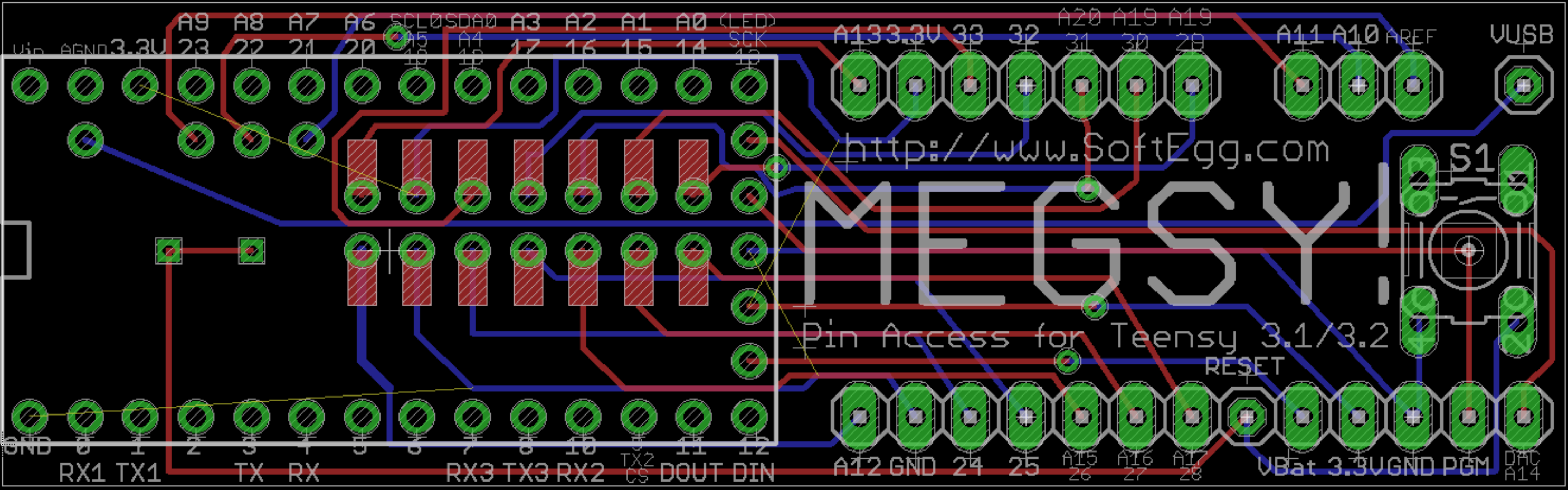 I haven't even really had a chance to use the protoboard version that I soldered up before, but I had a brainstorm and CAD'ed up this PCB.
 Here is the plan:
You tin the pads on the Teensy with solder, and tin the pads on the top of this board. Put all the headers on and slide the teensy ALL THE WAY DOWN, so the pads on the teensy are actually resting on the pads on this board. Then, flip it over and heat the vias with your soldering iron. Hopefully, the solder on the other side will melt and make a nice connection with the teensy board without bridging any connections. It's sort of a poor man's BGA! (That's ball grid array, for the layman).
There are a couple of nice design features I want to mention.
- I've added a reset button on this board so that, when the teensy is all covered up by the audio shield, you can still reset it. I also added a pin on the board for it. You can install that pin, or not, or even install it pointing up so that you can touch it with a ground lead if you like. This is set in two places for compatibility with Teensy 3.1 and Teensy 3.2.
- Another lovely feature is that I added the names of all of the pins around the edges, which should stick out around the edges of the Teensy on the top of the board. While the teensy is also labeled, this gives you a little more detail, calling out various feature pins like Analog inputs, TX/RX. I2C pins, etc.
This should give you access to 10 additional digital pins (6 of which can also be analog input pins), and 5 analog pins (one of which can be the 12 bit DAC output.) In otherwords, you can now work with everything not on an edge facing pin header. This should be handy when trying to use the various Teensy add-on boards like the Teensy audio board and/or the TFT display.
I'm sure, right about the time I finish this, Paul will release a real Teensy++ with even more features. Which is the preferred situation, really.
Discussions
Become a Hackaday.io Member
Create an account to leave a comment. Already have an account? Log In.