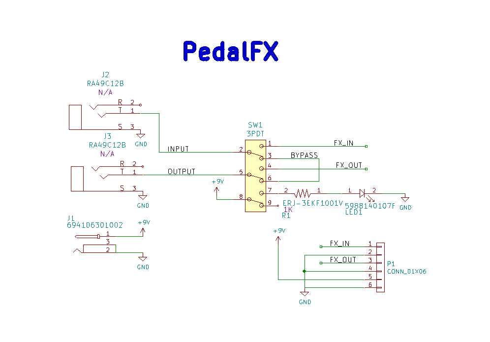
So a while back I mentioned I would be designing a PCB for making the process of taking and audio circuit and putting it inside a guitar pedal enclosure. The concept is inspired by the user mysticwhiskey, you can read more about his board in the project details section. The board is essentially the true bypass wiring that most guitar FX pedals use but as a compact PCB. My board is essntially the same except for moving the power input connector and using completely different components. My schematic is as follows:
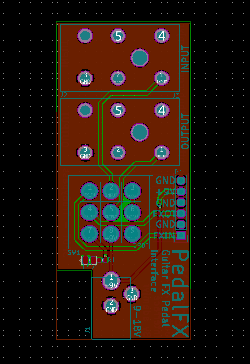
PCB:
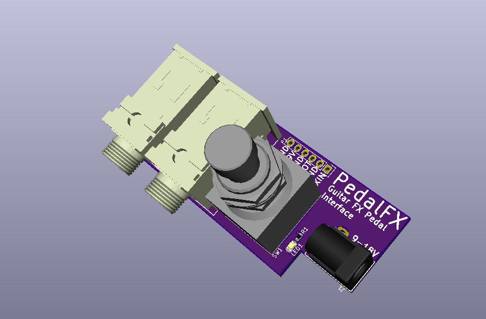
3D Views:
Top
Bottom:
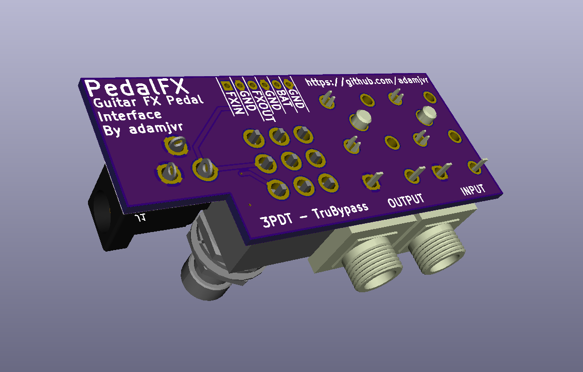
So its a fairly simple PCB but will make dropping these audio projects into guitar pedal enclosures super easy. The notch in the corner is geared towards aluminum hammond enclosures, this notch will allow the PCB to be tight up against the enclosure walls right in the corner maximizing space. The boards are gonna be made through OSHPark usng the 2 oz copper spec they offer, this will allow me to keep the board compact and make up for the trace witch limitations caused by the pad size on the 3PDT switch.
OSPark Renders:
Top Bottom
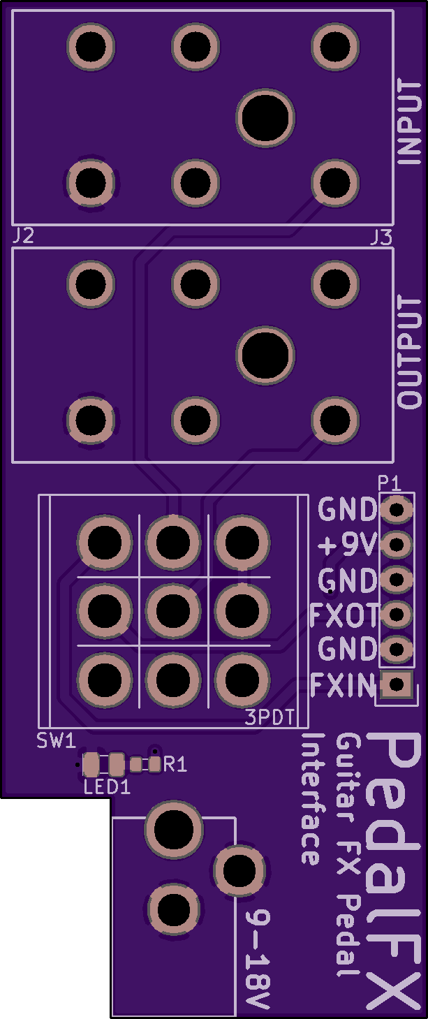
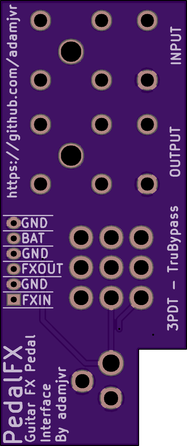
Thats all for now until I get PCBs in the mail. Stay tuned on the DT JFET Pre build and check out my other projects !
 AVR
AVR
Discussions
Become a Hackaday.io Member
Create an account to leave a comment. Already have an account? Log In.