DDL02 V7.1
See Part 1 of this log for details of the power supply circuit.
Gerbers
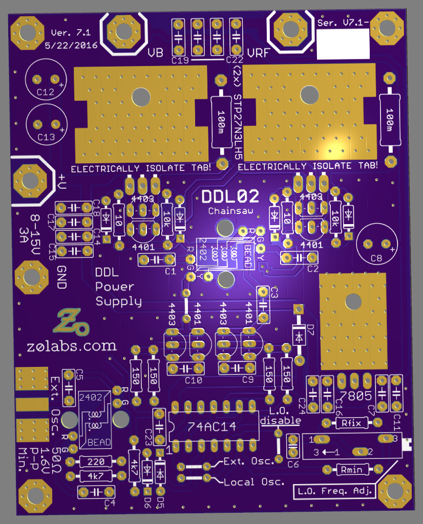
I started sharing the DDL02 V7.1 gerbers on OSH Park. V7.1 has an updated silkscreen and schematic with designators that match the other design files. In addition, designators are now on the silkscreen, so you know what to put where. After doing my own projects for so long, I got in the bad habit of not labeling the components very well. I'm trying to reform. Electrically, the board is identical to the V7.0 version I used on the clock.
Here's a render of the new version that I made using my in-house pre-flight 3D gerber previewer. This previewer software is on my list of things to open-source:
BOM
In the same spirit, I've created a detailed BOM for the DDL02. It's a google docs spreadsheet shared read-only (licensed CC-BY-SA). For some reason, formulas won't calculate for me - probably something to do with the privacy settings on my browser - so I couldn't make it quite as nice as I wanted. Once I get google docs working properly, I can revisit. I'd welcome any feedback on the BOM - I intend to make similar ones for the other boards, and would like to improve as I go.
There is one item on the BOM I'm not certain of yet. I wound the original transformers on Fair-Rite 2643002402 beads, and listed here the Laird 35T0501-10H instead so builders could order from one distributor. I haven't tested transformers on the Laird cores yet, but I'm waiting for some now, and will post an update once I have. The transformer windings should be bifilar (T2) and trifilar (T1) wound to reduce leakage inductance - you can find good tutorials on the web if you haven't wound one before. It's easy and rewarding: not too often do you get to make your own components.
Try not to substitute capacitors with lower voltage ratings. You might think that 50V caps in a 12V circuit are unnecessary, but ceramic caps have a nasty habit of exhibiting reduced capacitance as the voltage across them increases. If you substitute 16V caps instead, you may find a chunk of your capacitance has disappeared.
Q1 and Q2 must have their tabs isolated from the ground plane on the PCB beneath them. Here's the heatsink assembly as I built it:
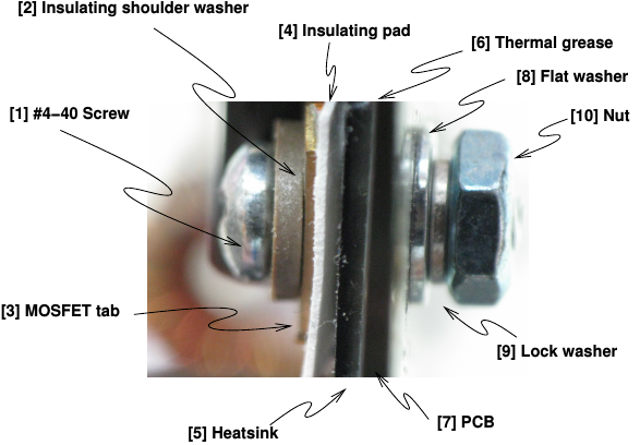
4-40 (or M3) hardware fits.
Design files
The Eagle design files are shared on hackaday.io.
Testing
OK, you built your first DDL02. Congratulations! Now, how do you know it works?
Here's what I did. I happened to have a bag of surplus 1.8 ohm 2W metal oxide resistors: 1.8 ohms is in the correct range to verify proper operation of the power supply. Unfortunately, a 2W resistor dropped across this power supply wouldn't last very long - so I made a 1.8 ohm 32W resistor using 16 of them. You could also use carbon composition resistors for this, but avoid wire-wound resistors of any type - they have far too much parasitic inductance. I run the fan over the resistors for longer tests. You can also test the supply with a stack of DDL01's, if you have them around.
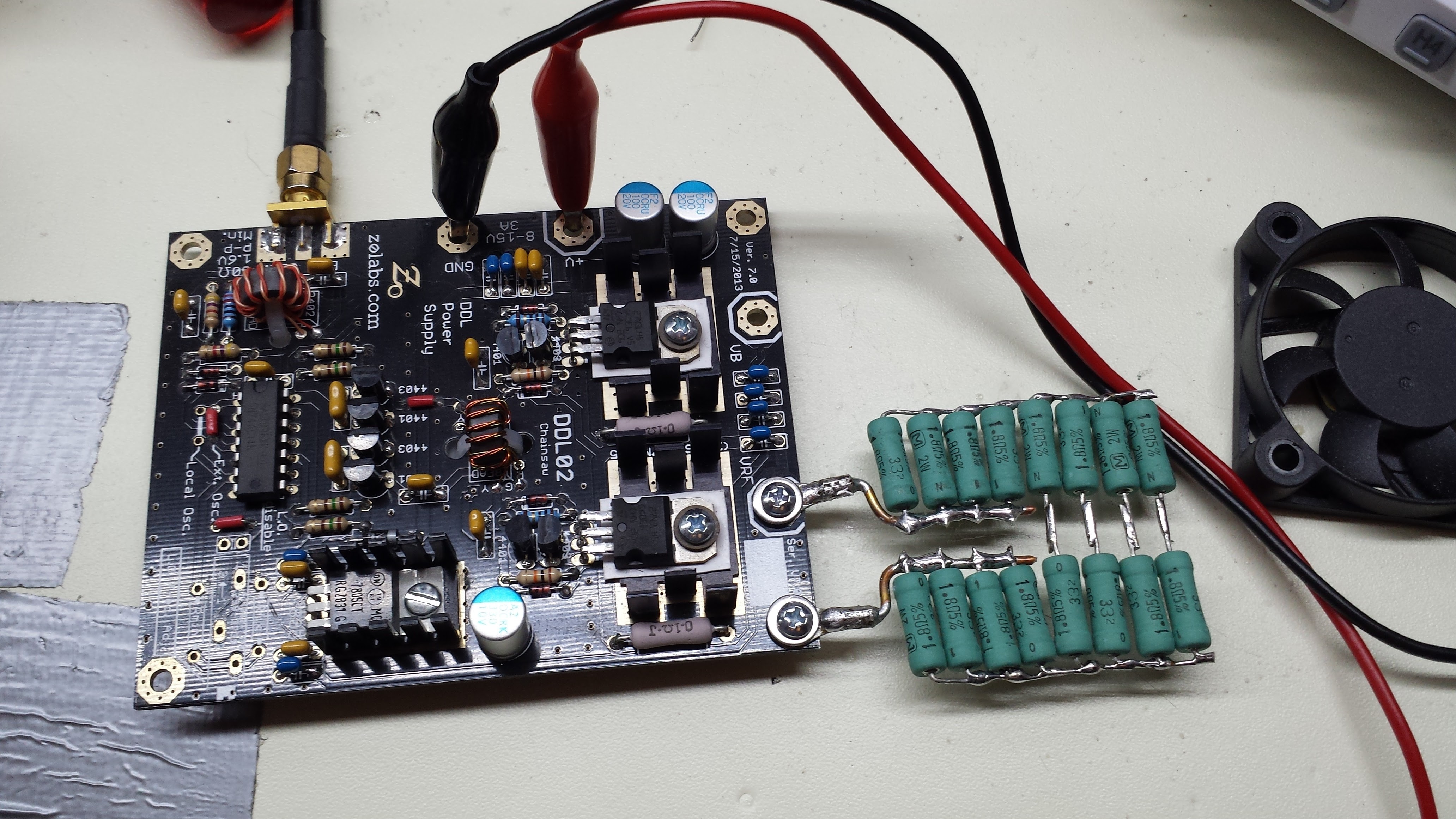
For testing, I initially started the "12V" supply at around 7.5 (a little above the 7805's dropout), and watched the current draw carefully as I proceeded. If you have a current-limited lab supply, this is the time to use it. I drove the input with a 3MHz +7dBm source ("TTL" output from a signal generator will work well), and slowly increased the supply to 12V. Current draw for this load at 12V and 3MHz is around 0.7A . Using a 10x oscilloscope probe on a 100MHz scope, you see the following output:
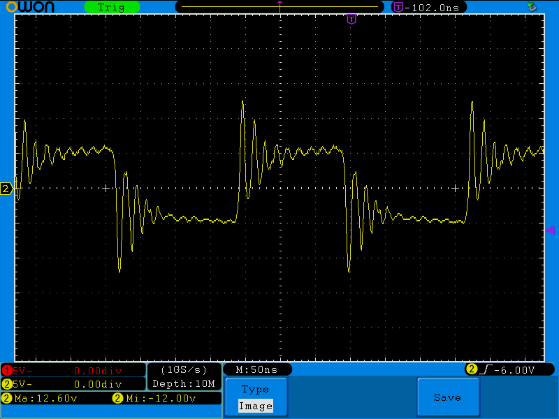
That ringing isn't bad probing - you see the same thing with a Z0-probe into a terminated scope input. Ringing like this is common with very fast MOSFET driver circuits (especially on through-hole PCBs - and on those designed by amateurs :-) The cause of and solutions to this problem are well-explained by Ti Applicaton Report SLPA010 "Reducing Ringing Techniques for NexFET High-Performance MOSFETS". There are two possible concerns here. First, the ringing excursions could exceed the Vds rating of the MOSFETS - in this case, the 24Vp-p excursions are within a safe margin for 30V MOSFETS. The second concern regards emissions. A quick look at the ringing shows it to be around 60MHz. While the size of the conductors in the clock don't make effective radiators for the 3MHz signal here, 60 MHz leakage could be an issue.
I'll note here that the DDL01 boards don't care about this ringing; they work fine either way.
To be a better EMI citizen, we can clean up the waveform with an RC snubber. Following the design procedure outlined in the Ti document, I first tried a 100pF capacitor in series with a 13 ohm resistor across the output:
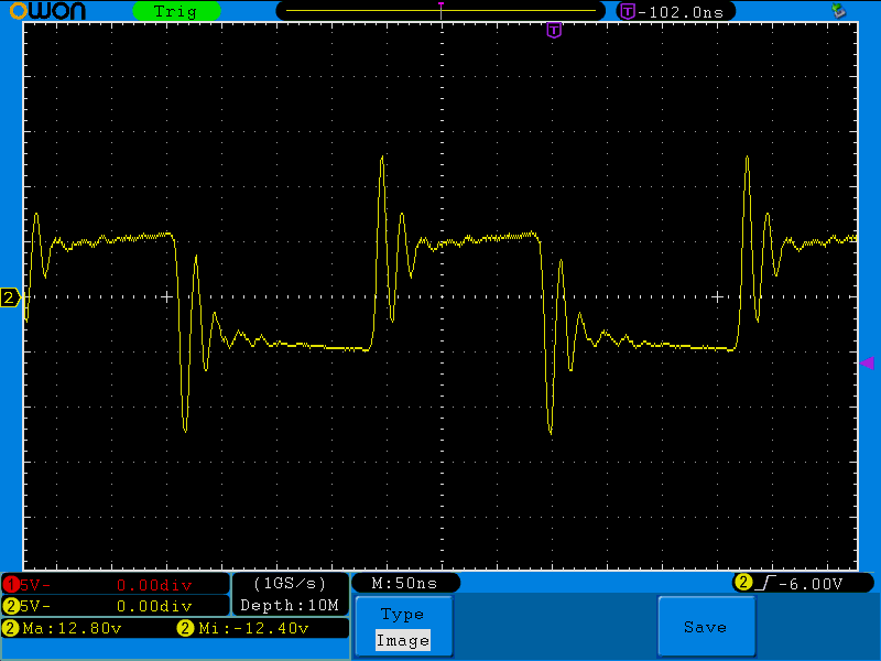
Definitely better, but still not great. I tried a few other combinations before settling on a 220pF/10 ohm snubber, which resulted in the following:
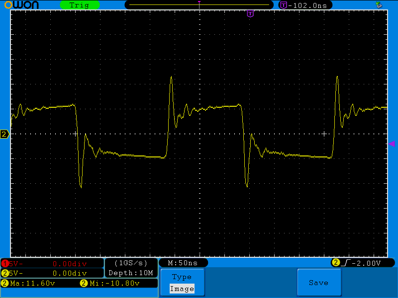
now, the initial excursion is still there, but the 60MHz energy is damped pretty well.
There aren't sites on the current rev of the DDL02 board for the snubber components - they are better off determined experimentally when the board is attached to the desired load. The series RC circuit can then just be wired conveniently across the Vrf and ground terminals on the DDL01.
Thermal Issues
For a long time, I thought the power devices ran too hot on the board. This was based on the age-old "finger test" in which the engineer sticks his or her finger inside running equipment to verify design calculations. I have subsequently purchased an IR thermometer and now think my finger must be out of calibration. The MOSFETs and 7805 show peak temperatures of 45-50 C (on the outside of the package, anyway). They're probably OK.
 Ted Yapo
Discussions
Become a Hackaday.io Member
Create an account to leave a comment. Already have an account? Log In.