When working out the component layout, one of my major goals was for this project to be compact and pocket-sized. Therefore, as a rough guide, I figured that it shouldn't be larger than a phone.
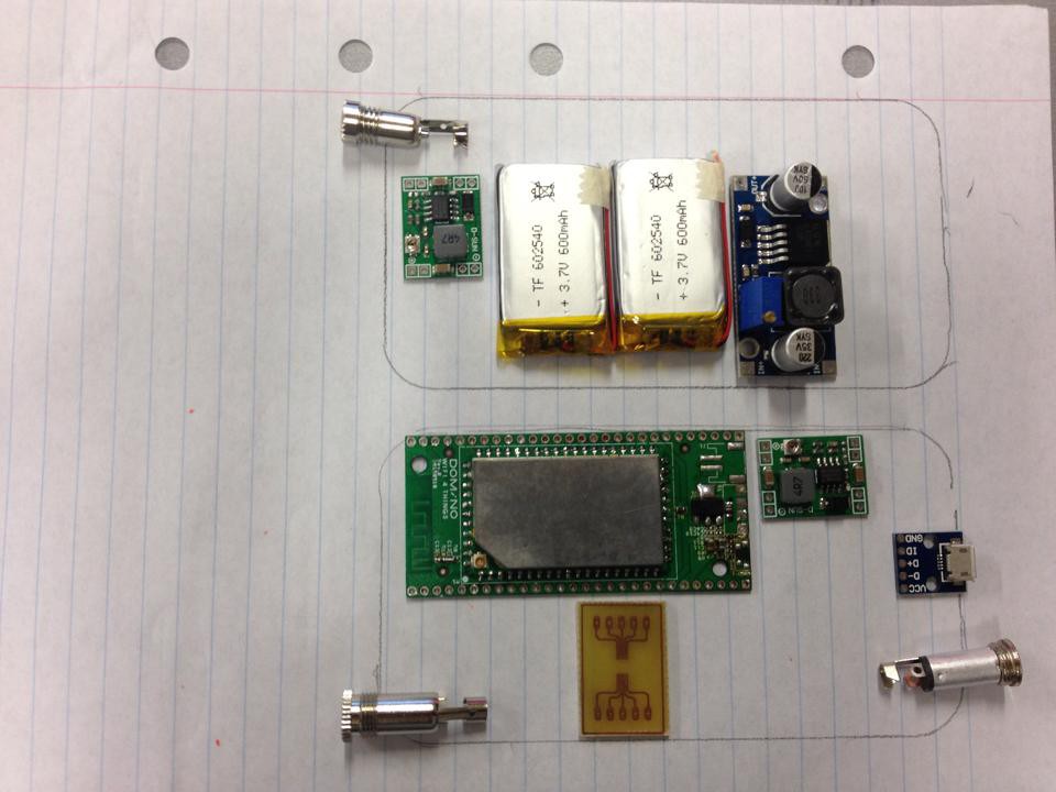
I started by drawing the outline of my phone and trying to place the components within it. Looking at the schematic, it made sense to put all the power supply and amplifier components in one section, and have a separate section for the ICs and audio jacks. Since the parts are all very thin (with the minor exception of the boost converter), I separated them into two layers.
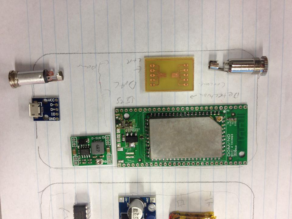
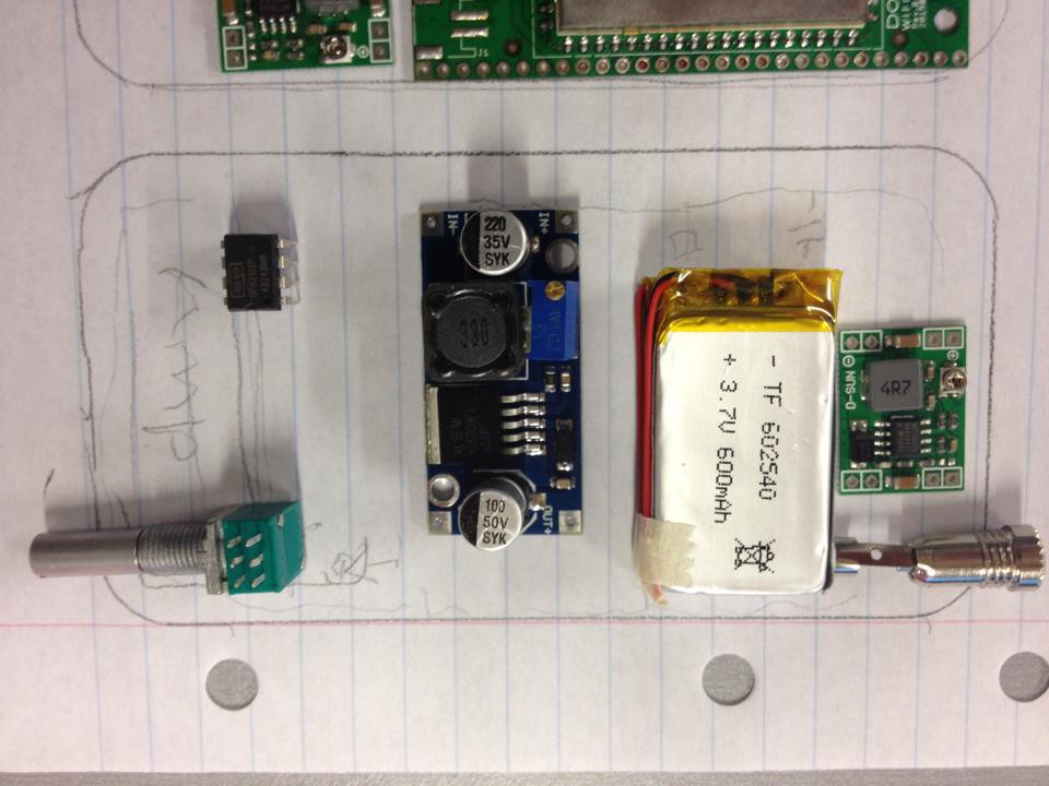
I tried out a number of different arrangements, trying to make parts linked in the circuit diagram close together.
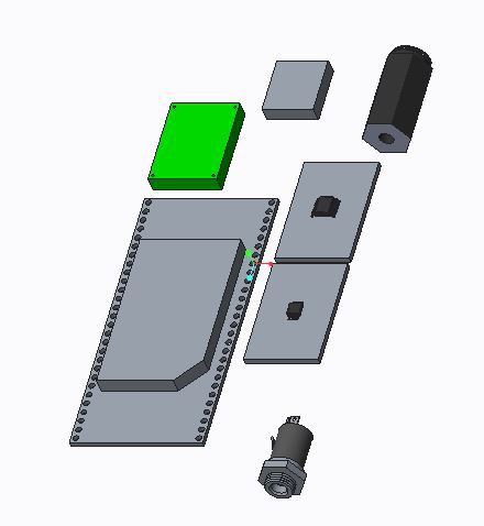
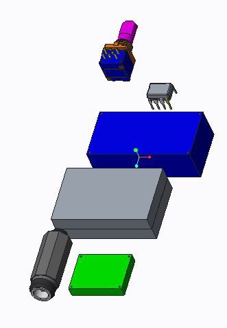
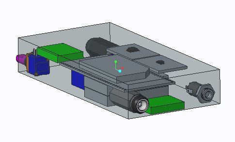
Finally, I modeled the arrangement using CAD. For this application, I used PTC Creo. I made sure that the outside dimensions were correct, to ensure that there would be no collisions, but I did not produce parts with fine-detail. Where possible, I used the manufacturers' CAD models available online.
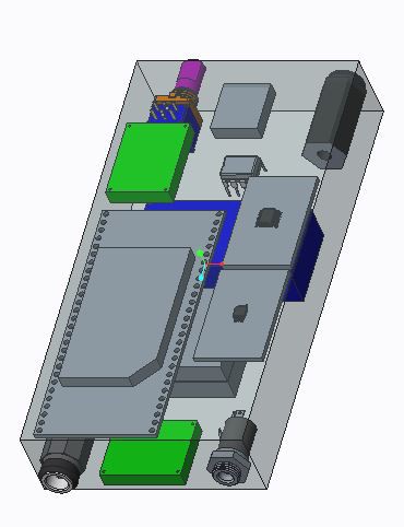
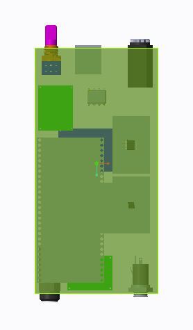
This is the layout of the top layer. This consists of the single-board computer, voltage regulator (green) supplying 5V, the DAC and Audio Switch ICs on breakout boards, the micro USB port for digital audio in and the two 3.5mm audio jacks. One (at the top of the picture) for audio out and the lower one for bypassing the digital stages and using the amplifier directly. Space has also been to implement the detection circuit.
The bottom layer contains the barrel connector for charging and external power supply, a voltage regulator (4.2V), two batteries stacked on top each other, the boost converter (in blue) and the amplifier components: the volume control dual potentiometer and the op-amp.
The final series of combined assembly images should make it easier to place the components in the pocket-sized enclosure during manufacture.

Discussions
Become a Hackaday.io Member
Create an account to leave a comment. Already have an account? Log In.