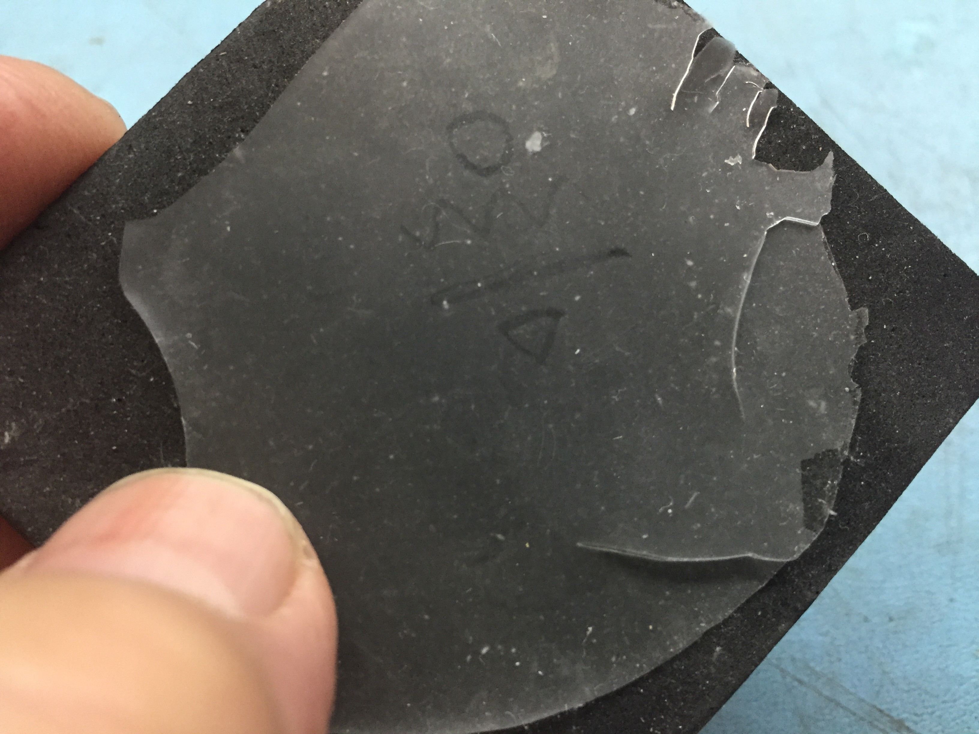
I know for some it might be a bit underwhelming to see a few picture taken of a piece of silicon rubber with what appears to be an image of a few lines in relief. However for others it may well be the freakin holy grail! So show a little respect:)
Amazing how little bits of dust get picked up, seemingly out of nowhere. You'll note that from the previous log the parts of the line that were the darkest blue, are now the darkest black which suggest those sections are the thickest. I'll have to add a profilometer to the list of instruments that need to be built. I would think, that the depth of the relief is no more than a few microns.
Incidently, the PDMS pealed off the alumina substrate easily. Perhaps it wasn't clean enough. Like most things made with silicone compounds, not much, including itself sticks to it. If it isn't in the first pour, and you don't have a plasma ozone etcher, then "Forget about it".
 Chuck Glasser
Discussions
Become a Hackaday.io Member
Create an account to leave a comment. Already have an account? Log In.