Close
0%
0%

Affordable Spectrum Analzyer

Analyze electrical signals using a raspberry pi with a user interface designed for students, hobbyists, and other beginners.

Similar projects worth following
Spectrum analyzers provide a visual aid to circuit design and signal processing critical to troubleshooting and understanding how frequencies both affect and are affected by electronics. While the educational and practical applications of such devices are extensive, the availability of such devices are often limited by cost and usability. Similarly, low cost designs often suffer from lack of range or resolution. Our design overcomes cost and limited usage by implementing a hybrid superheterodyning and fast fourier technique. The superheterodyning aspect grants the device a robust range while the fast fourier and digital calculations allow for imperfections in devices to have lower impact on the signal integrity. Additionally, cost and availability were made more attractive by using the Raspberry Pi, a widely available and low cost computer, as the central controller of the system.

The spectrum analyzer is an incredibly useful tool for any person dealing with signals. They allow us to see something a bit abstract, but quite useful: signals in the frequency domain. This has a variety of applications, such as radio, audio, and circuit analysis. Anything problem that can be solved by better understanding the spectra of the signal is the domain of the spectrum analyzer. My original fascination with these devices came from watching the spectra of the audio band for my favorite songs. I loved the visualization of the high notes and low notes in the spectra. This has inspired me to try to create devices like this in the past, though not full solutions. This project was chosen to finally create an all-in-one solution to a spectrum analyzer. The bonus is that we have found this project to be an exemplary review in all of our electronics learning. Everything from signal analysis to circuit design is heavily involved in this project. We ultimately want to create a product we would want to use. And we know we are not alone in this desire, so we are going to create a spectrum analyzer that is at a cost that is attainable by the hobbyist and the student.

Equipment for analyzing electrical signal spectra is inherently expensive. Equipment typically runs on the order of $50,000, with lower-end devices still costing on the order of thousands of dollars. Though expensive, these devices offer high resolution and operate in a wide range of frequencies. This is great for industry, where precision may be key, but the functionality is often over-kill for educational, hobbyist, or professional audio usage and the prices are likewise impractical. In addition, the user interface for many devices are hard to use, assuming the user has a working knowledge of spectrum analyzers, and requiring tuning and calibration. This combination makes spectrum analyzers inaccessible to hobbyist and audio electronics communities and a financial burden on educational institutions not requiring industry precision.

Inexpensive spectrum analyzers, costing under $500, do exist, albeit in smaller quantities than their more expensive counterparts, but do not remove the learning curve associated with the devices. The project proposed is a stand-alone low-cost spectrum analyzer, with a built in display, that supports a simple user interface. The physical device will be able to detect frequency spectra in addition to calculating total harmonic distortion and measure frequency domain noise. The interface will take advantage of presets, built calibration and tuning and intelligent parameter selection so user with limited knowledge of the device could easily utilize it. More advanced parameter settings will be exposed to the user as well for finer-tuned usage and to appeal to the more knowledgeable user.

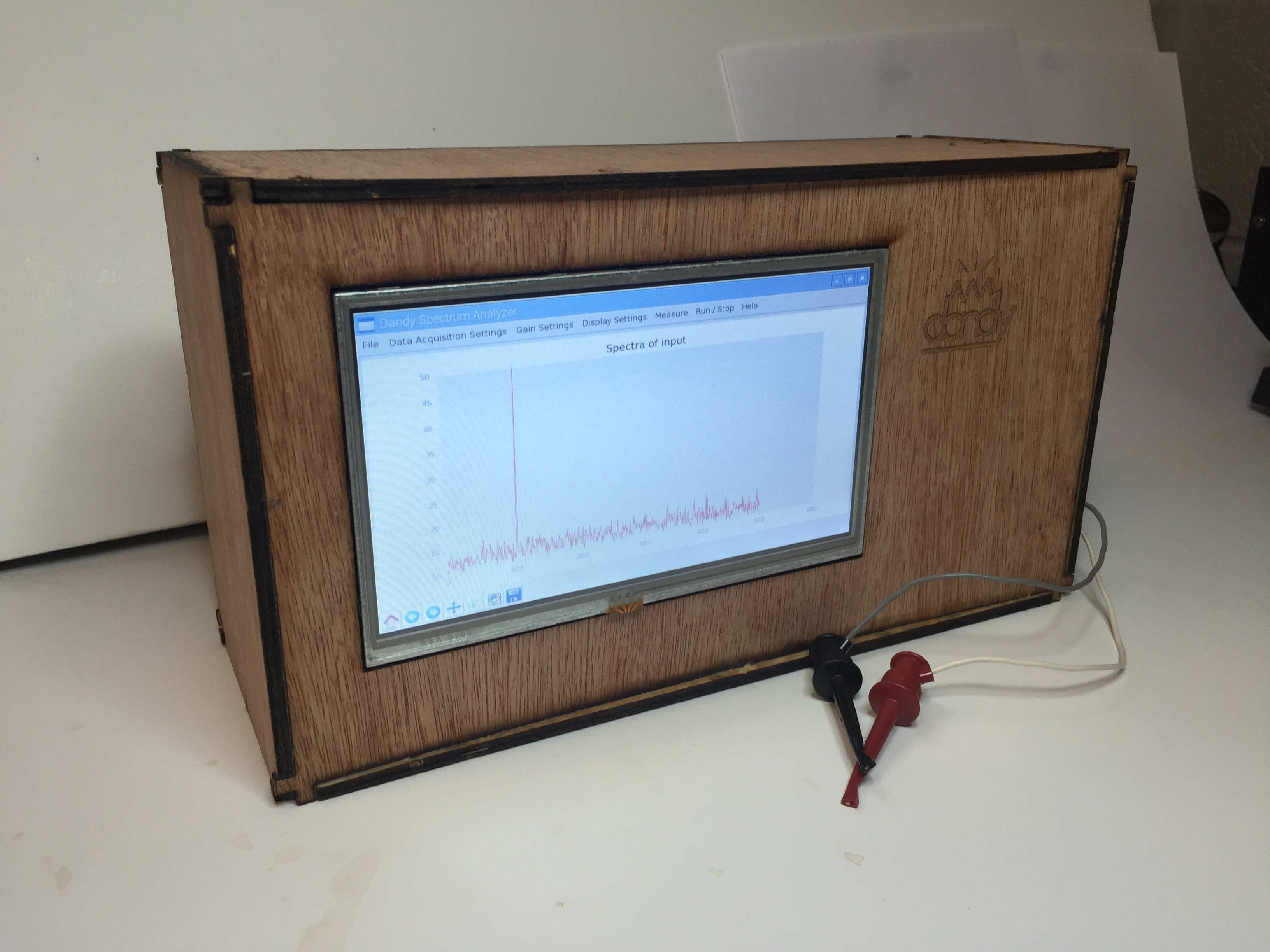
Below is a working prototype of our project.

View all 23 components

  • Testing out the Spectrum Analyzer and Getting Results

    Dan Kisling07/10/2016 at 23:59 0 comments

    It's the log we've all been waiting for. I've been hand wavy all this time. Does any of this stuff actually work?

    Of course, at first, no. None of it worked. Everything was broken. Or maybe that's just how it seemed. But by the second revision of the board and the um-teenth revision of the software we got somewhere. Here's one of the first tests we did of the spectrum analyzer. I did it in my dorm room late one night. Since it was just my room, we improvised for a few things. Instead of a nice lab grade function generator, we used a function generator app on my cheap tablet using the headphone port. The D/A on that tablet is kind of crappy, so were not paying that much attention to every detail, we are most interested in seeing if the frequency that tablet says close to that of the spectrum analyzer. You can't tell that much from the video, especially due to the lighting, but you can see the peak frequency move from right to left as the frequency increases on the tablet (and is simultaneously being shown on an oscilloscope on the right).

    From there we did a few improvements, and more tests - this time using a lab grade function generator. Here's a video using our superheterodyning technique signal path. In this setup our maximum frequency we can see is 100kHz.

    Here's another video, this time bypassing the multiplier and bandpass filter for a simpler input scheme. This design allows us to see signals up to 500kHz.

    We have tested the alternate design with signals up to 500kHz with large success. Below are plots made and saved by our spectrum analyzer for different signals provided by the signal generator in lab. Sine wave inputs give us a good view of how accurate our frequency measurements are. In each of these tests, we have the spectrum analyzer determine the frequency, which should be accurate to 124Hz (1MHz / 8092 Samples). Square wave inputs give us a good idea of signals with a wider spectrum and allow us to see if there are any aliasing problems. In the alternate design, this should not be an issue as the signal is just fed from an input amplifier straight to the analog to digital converter. The square wave test (which is done without changing the frequency setting on the signal generator) also allows us to see the consistency of the determined fundamental frequency by the spectrum analyzer. The square wave test will become more important in the full system design.

    Spectrum Analyzer Capture: 5kHz Sine Wave Input

    Spectrum Analyzer Capture: 5kHz Square Wave Input

    Spectrum Analyzer Capture: 20kHz Sine Wave Input

    Spectrum Analyzer Capture: 20kHz Square Wave Input

    Spectrum Analyzer Capture: 56kHz Sine Wave Input

    Spectrum Analyzer Capture: 56kHz Square Wave Input

    Spectrum Analyzer Capture: 450kHz Sine Wave Input

    We have also tested the full design with similar success. One issue that arose during test of the full signal path design is the accuracy of the frequency reading. The reading was pretty consistently off by about 2kHz. Since we knew the alternate design was performing correctly, the 2kHz offset must be created by an element introduced in the full system design: the multiplier, the oscillator, or the band pass filter. The band pass filter and multiplier options did not make much sense, so the oscillator looked like the culprit. Looking in the data sheet, we realize that the oscillator has 0.5% initial accuracy, which seems low until you realize that 0.5% of 455kHz is 2.275kHz.

    To test our suspicions, we used the alternate design to probe the output of the oscillator. This would allow us to see the spectrum of the oscillator and easily determine exactly what frequency it was operating at. The oscillator is supposed to operate at 360kHz, 370kHz, 380kHz, 390kHz, 400kHz, 410kHz, 420kHz, 430kHz, 440kHz, and 450kHz. Below are select captures of the spectrum when varying the frequency setting on the oscillator.

    Spectrum Analyzer Capture: Oscillator set to 360kHz

    Spectrum Analyzer Capture: Oscillator set to 390kHz

    Spectrum Analyzer Capture:...

    Read more »

  • Enclosure

    Dan Kisling07/10/2016 at 23:25 0 comments

    For this project I designed my first enclosure. Up to this point I had been carving cigar boxes or cutting cardboard boxes. I had already done some 3-D prints up to this point, but I thought a 3-D printer was a poor choice for this enclosure. After all, I basically want a large box to stare at. 3-D printers are much better suited for smaller more intricate designs in my opinion.

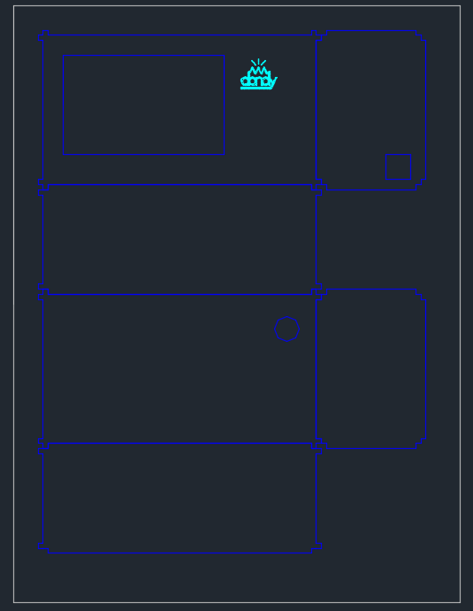
    So for this project I chose laser cut my enclosure from plywood. I've always wanted to learn how, so this seemed like a great opportunity to try it out. I still cheated to create the design, as we were under tight deadlines, and I didn't really know my way around Autocad. I used a python script to create a tabbed enclosure (I believe this is where I got it). From there I edited it to include our logo (my graphic designer friend helped me create the file), and cutouts for the screen and some cables and switches. I sent it off to our design labs on campus to create it and within minutes I had it all laser cut.


    Link to enclosure I designed here (github).

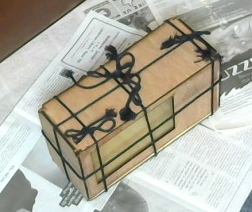
    Below is a quick video of me gluing it together. I just used some wood glue and tie line (since that's what I had on hand.


    I left off the back panel that way I can get inside. Lucky for me, the wood was warped in such a direction that the back panel fit snug inside without any glue or screws. Here's a picture of the enclosure with the screen inside. I used some cheap M2.5 screws and nuts to attach the screen.


  • Software

    Dan Kisling07/10/2016 at 22:17 0 comments

    In this log we'll focus on all of the software. Most of the logs so far cover stuff that could be developed or done in a week or two. This log is very different. The one piece of software (the device driver) alone took most of the academic year to develop. All of the software was developed by my lab partner and local genius, Andrew. That is, with the exception of the GUI: I wrote that.

    The software developed for this project is divided up into three parts. The software is broken into three separate systems, the driver, the controller and the user interface. Each sub-system is responsible for a different task and is separated by operational priority. The driver, interacting directly with the Raspberry Pi hardware, has the highest priority, requiring accurate timing and as-fast-as-possible computing time for consistent sampling. The controller has the next highest priority for processing time as it responsible for computing the fast fourier transform and reconstructing the segmented spectrum. At the lowest priority and least mathematical computations is the user interface, responsible for plotting the spectrum and interacting with the user.

    Device Driver

    Github link to code for driver, and header file.

    The purpose of the device driver is to provide an interface between the hardware and the higher level software. The driver is responsible for physically writing out SPI commands to the local oscillator, physically changing the pin levels for the amplifier, setting up and altering the sampling clock, and reading in the input bits from the ADC. In order to accomplish this level of control, the driver is written as a linux kernel module for both a character device and SPI device.

    The character device aspect allows the board to be interacted with like a normal file in software would. Namely, the driver allows the device file to be opened, read, written to, memory mapped and closed in order to interact with the physical bored. Opening the device opens a channel for interacting with the driver, similar to opening a text file to edit it. Reading the device prompts the driver to take samples for a predetermined number of samples and step the local oscillator a predetermined number of steps, storing all results in a 1 MB buffer in kernel space. Kernel space is a separate region in memory, distinct in the linux operating system, which is reserved for low-level hardware and driver interaction. In order to use this data, memory must either be copied into user space, where user applications run, or it must be mapped there, Since the user interface runs in user space, the driver allows for portions of the data buffer to mapped using memory mapping. Writing to the file allows for the driver’s internal values to be modified, For example, the local oscillator steps, sampling frequency and amplification level can all be changed by writing to the driver. To facilitate this, all data must be formatted correctly, so the driver can interpret the changes correctly. Finally, closing functionality closes the channel safely, similar to saving and exiting a text file.

    The functionality not exposed by the character device are the initialization and cleanup of the device. During initialization, all memory buffers are created, the GPIO pins are formatted to their expected operation and the sampling clock is set to the correct frequency. This guarantees that if the system were to change from other software on board, when the device starts each time, device is in a known and guaranteed state. The cleanup functionality reverses the effects of the initialization so the board returns to a state that is not utilizing resources unnecessarily.

    In addition, the SPI interactions are logged as a separate device and driver, following the SPI driver interface. The device itself does not expose any SPI interactions with the user, but utilizes them during sampling, thus it is necessary to register a secondary driver. This driver purely handles unidirectional communication from the...

    Read more »

  • Board Assembly

    Dan Kisling07/10/2016 at 21:48 0 comments

    Just for fun I thought I'd upload a quick video of me assembling the board. Please excuse the blurry video attached.

    Before this year I had never worked with SMD parts. My advice, it's really a lot easier than you think. Just get yourself a SMD rework station. Mine is a cheap Yihau and I love it.

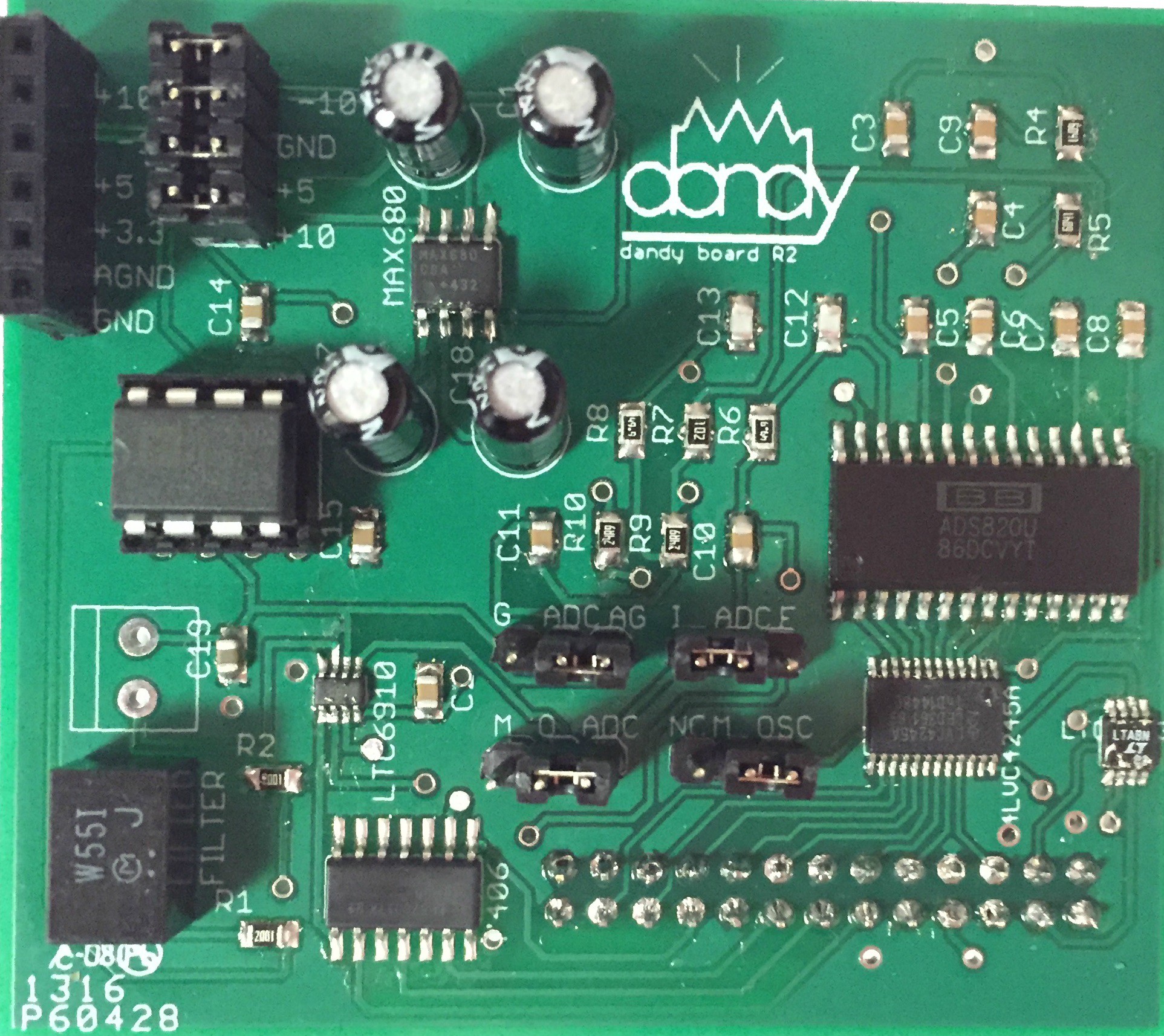
    Below is a picture of the board once assembled.

  • Hardware

    Dan Kisling07/10/2016 at 21:35 0 comments

    Skipping ahead now to hardware. My focus on this project was the hardware (Andrew focused on the much harder subject: software). This project log will be quite lengthy, and only really considers our second revision of the PCB. The first had a whole host of issues (and it was my first PCB I ever designed). Many issues were corrected in the second PCB, but there are still a few improvements I would like to introduce in the near future.

    Hardware Selection

    Multiplier

    The multiplier considered are listed in components. We found that the low cost multiplier used in the electronics lab (AD633) was sufficient, and actually had some frequency properties that made it a good choice for this project.

    Band Pass Filter

    A very tight band pass filter is required for the design to function properly. As such, a band pass filter with middle frequency 455 kHz and 10 kHz bandwidth was selected. These already exist, have impressive brick-wall-like transfer functions, are inexpensive, and require no additional power considerations. The specific part chosen was the CFWLB455KJFA-B0 from muRata. Note that it requires a 2KΩ input and output resistance.

    Oscillator

    The variable oscillator chosen needs to be variable, easily controlled digitally by the Raspberry Pi, and low cost. Our simulations were able to show that multiplying signals by a clean sine wave was not necessary. In fact, we can get away with square waves as the images from the harmonics are separated sufficiently and filtered out by the band pass filter. The LTC6903 from linear technology was chosen for all of these reasons. It is able to produce square waves from 1kHz to 68 MHz with no external components. Communication is handled via SPI protocol, and the Raspberry Pi has dedicated SPI GPIO pins.

    ADC

    The analog to digital converter chosen needs to be able to work with specific sampling frequencies in order to achieve undersampling methods described above. For our purposes, we desired a parallel out digital signal so timing of communication would not complicate matters. Additionally, a track and hold topology is beneficial as it simplifies our circuitry and does not require an external sample and hold circuit. Considering all of this the ADC chosen is the ADS820U from Texas Instruments. Interfacing with the IC is simple. All that is required is a bit of signal interfacing, a clock signal, and the digital bits are provided at the output. As this ADC is 5V logic, a level shifter is required at the output to convert to the Raspberry Pi’s required 3.3V logic. The 74LVC4245A is chosen to do this as it can handle 8 bit level shifting at sufficient speeds, comes in a small package, has simple setup, and is low cost. A level shifting is required for the input clock signal as well, but this time 3.3V to 5V. This is a simpler operation, and so the extremely low cost 7404 hex inverter / buffer is utilized. The inversion of the clock signal requires no reprogramming as we are only concerned with signal frequency, not phase.

    The ADS820U requires a good bit of interface circuitry. The components and connections are taken from figure 5 and figure 10 of the datasheet as an AC-coupling topology is preferable to our application as we are really only concerned with AC signals and allows us to neglect DC biasing to fit the ADC range.

    Input Amplifier

    The input amplifier needs to have a sufficiently high gain bandwidth product, and it is desireable to have an easy interface to control the amount of gain. Linear Technology’s LTC6910-1 is chosen. An added benefit of this IC is its ability to be powered by a single sided 5V supply, something the Raspberry Pi can do without any additional circuitry.

    Power

    Finally, the power is considered. With the exception of level shifter and the multiplier, every active component on the circuit is powered by the 5V power line from the Raspberry Pi. The level shifter also requires a 3.3V input (so it knows what level to shift to). This 3.3V input can also be supplied by the Raspberry...

    Read more »

  • Simulation

    Dan Kisling07/10/2016 at 21:09 0 comments

    In this log I'll describe the simulation Andrew and I created to verify our sampling technique. Simulation is powerful technique that allows us to create our circuit and see how well it works. It allows me to make changes to our system quickly and efficiently to see their effects. Even faster than breadboard testing.

    To prove that our signal capture technique would work, a few different matlab simulations were created. The first simulated our entire system, allowing us to “probe” signals along the signal path. A second simulation was created to validate our idea about eliminating the second oscillator. The results of the second simulation were then integrated into the first to create a full system that tested the viability of our system. The simulation modeled our sampling method, analog manipulation, and FFT algorithms. In this simulation an input spectra (up to 100kHz) is created and the system breaks the spectra into ten windows of 10kHz each using our method. The bandpass filter implementation is with the actual transfer function of the filters, so it can realistically show how the filter will actually act in the circuit. The oscillators are perfect cosine waves, but can easily be modified to be not ideal in order to understand the effect of a real IC oscillator. The sampling is simulated by a function that only takes every few points from the output and then computes an FFT on that signal. The output of the simulation is included with analysis below.

    Plots from Full System Matlab Simulation

    The above waveforms shows (top) the input spectra into the system. This is a bit random but it is important to test frequencies near the edge of the window (at 10kHz increments). Below are ten smaller plots, which show the system’s response to the input at different frequencies of the first local oscillator. As the local oscillator decreases (in 10kHz steps) different sections of the original input spectra are pushed into the region of the bandpass filter and are thrown back into the baseband by two different means. The simulation does this by either using a second oscillator or through undersampling. Though some digital manipulation, these 10 windows are then spliced together to create our final window, a recreation of the input spectra. We see in this simulation that we are able to restore the original spectra with no aliasing. This was true for both the case using the second oscillator and that of undersampling. The only noticeable difference between the top spectra (input) and bottom spectra (output) is a scaling to the amplitudes, which can be corrected by inverting the transfer function of the bandpass filter in digital processing. The main takeaways so far are the relationship with the actual sampling frequency and the ability of the system to produce an output without any aliasing. So far we have found that a sampling frequency of 110kHz will produce these results. We are pleased with this result as we have read of methods to input data into the raspberry pi with sampling frequencies much higher than these. In addition, 110kHz is less than the 200kHz that would normally be required for a sampling frequency of a signal that extends to 100kHz. To further that goal of extending input frequency, not causing aliasing, and minimizing sampling frequency quadrature filters are considered and simulated.

    As a final note on the simulation, it was determined that the band pass filter used in the simulation would actually distort the signal too much, was costly to build, and added a great deal of complexity. Instead, a pre-packaged band pass filter was found that was originally designed for radio at 455kHz. We knew that we could rearrange the oscillator and other spacing to make this frequency work. The added benefit is a near-brick-wall band-pass filter that is low cost and very reliable.

    Our full matlab code can be found on github.

  • System Block Diagram

    Dan Kisling07/10/2016 at 20:09 0 comments

    Let's jump into the simplified system block diagram for our spectrum analyzer. What is posted below is actually our revised system block diagram. Our first diagram had a few components we decided to eliminate, and while it is good to learn from our mistakes, it is also good for to avoid writing a novel on how to build a spectrum analyzer.

    To elaborate further on the picture, the differential signal comes in through probes to a digially controlled amplifier (so the user can increase the gain in order to see smaller signals on the device). From there it is passed through a digitally controlled oscillator. We used the LTC6903 as it was easy to use. Astute readers might point out that in the last log I said sinusoidal signals, and the LTC6903 produces square waves. They are correct, but a square wave is just a sine wave with extra harmonics. As long as the harmonics don't distort what you're doing (as they are eliminated by the bandpass filter) why not use square waves. We found that square wave oscillators were easier to control and cheaper to buy.

    After the signal is multiplied by different frequencies it goes through a really sharp bandpass filter. This bandpass filter is awesome. We tried to design our own, but found it was really hard to not significantly distort the signal. Our adviser suggested we look to see if there was a cheap part built for AM radios that could work for us. And sure enough, for a couple bucks you can have a really impressive passive bandpass filter. I mean, check out the frequency response to this thing. It's about as close to a brick wall filter as I've ever seen.

    After the bandpass filter, the signal is sampled by the ADC. Everything from there is done in software. The raspberry pi takes the samples and performs a GPU accelerated FFT on them, splices the spectrums together, and displays them in the GUI to the user. The user can then use the GUI to change some settings in order to capture the signal he or she wants.
    I'll elaborate more on this point when I discuss the hardware design, but we also broke out a second signal path in our PCB. By moving some jumpers, you can get the signal to come straight from the digitally controlled amplifier straight into the ADC. This allows someone to sample a signal in a straight forward manner, without all of the superheterodyning fanciness.

    That's all for now. In the next log I'll talk a little bit on simulation of our technique to test its feasablility.

  • Superheterodyning Technique

    Dan Kisling07/10/2016 at 19:40 0 comments

    This log is going to get a bit more technical than some of the other logs. Don't get discouraged from the language or the techniques used. The more sophisticated input method (spoiler alert) turned out to be not as good as the simple one. This log is here to describe this superheterodyning technique to those who are interested. By no means is this log entry something that needs to be understood in order to build your own spectrum analyzer. I find this stuff interesting, so I included it for others who might feel the same way.

    Let's start this log by talking about sampling. Nyquist sampling states that we need to sample at least twice the frequency of the highest frequency we want to capture. Or, at least, this is how most people understand Nyquist sampling. But the truth lies within the details. In fact, you need twice the frequency of the total bandwidth you would like to capture. To explain this point, lets talk about a 10KHz bandwidth signal starting at 150kHz. So that signal lies completely within 150kHz and 160kHz. One might believe that you would need to sample at 300kHz minimum in order to capture the signal without aliasing, and they are correct. If you sampled at 100kHz, for example, and you just displayed your FFT from 1kHz to 100kHz, you would see your signal (backwards) from 40kHz to 50kHz. But there's something magic to that: we actually did capture all of our information, it's just in the wrong place and backwards. We would get into trouble if we had a 60kHz bandwidth, as the signal would fold on itself when sampling at 100kHz. But as long as our input bandwidth is low enough and we know how to correct the signal, we can use this to our advantage.

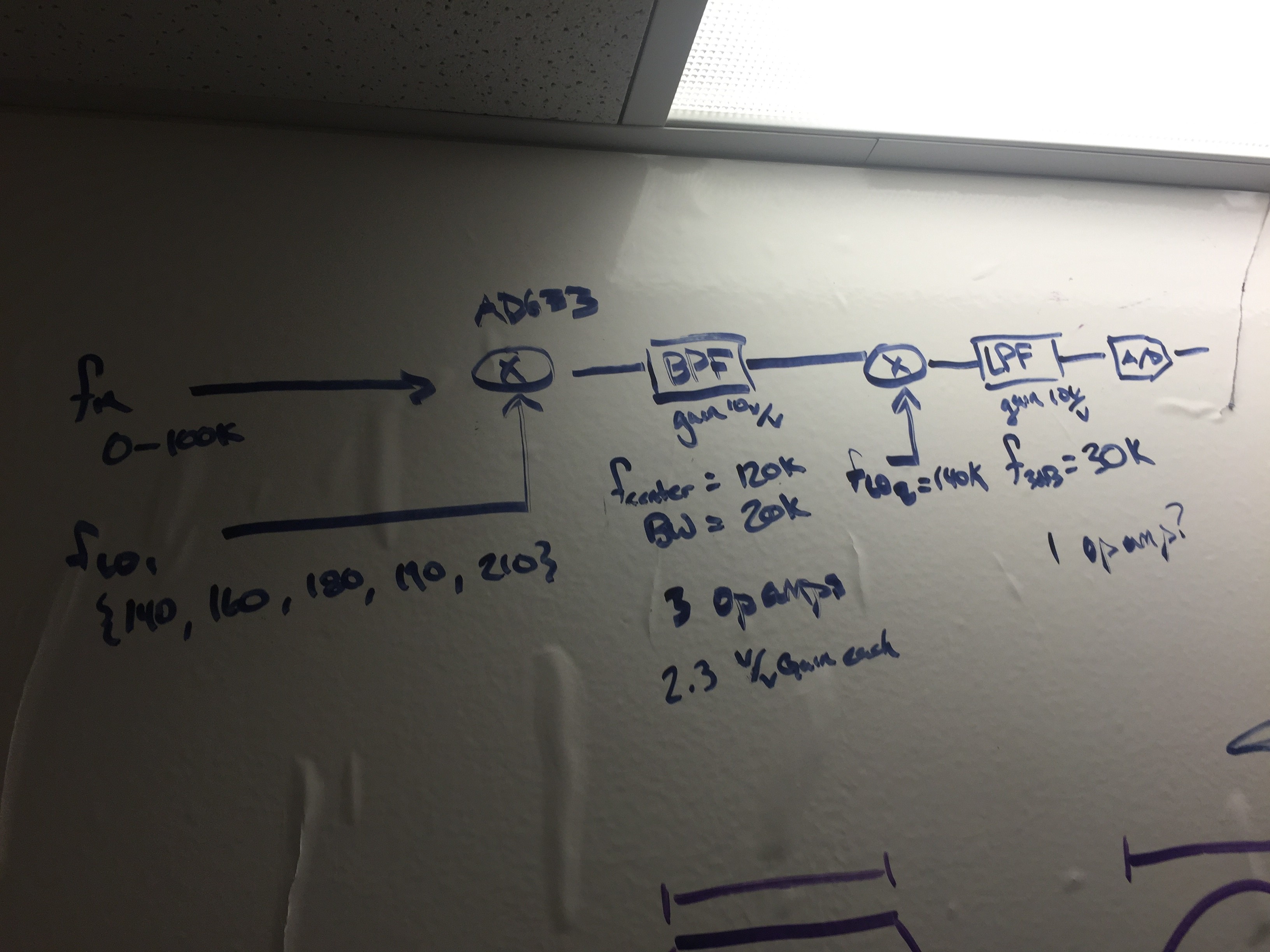
    This is where we get fancy. Now lets multiply the input signal by a sinusoidal oscillator. This effectively allows us to move our signals frequency in the frequency domain. Add into the mix a very sharp band pass filter. With these two elements, we can take a large bandwidth and section it into smaller bandwidths. For example, take a 30KHz bandwidth signal. Multiply it by a sinusoid at one frequency (we'll end up calling this a local oscillator), and then pass it through a 10kHz bandpass filter (the filter always filters the same frequencies), and then sample it. Then change the local oscillators frequency by 10kHz. Run that signal though the same bandpass filter, and then sample it. Finally, move the oscillator one more increment of 10kHz before placing it through the bandpass filter and sampling it. What we have done is allowed ourselves to take a 30kHz bandwidth signal, and sample it 3 times and each time we just need a 10kHz bandwidth requirement in order to fulfill our Nyquist criteria. There is a great deal more I could say about this matter, such as the particulars about the filters and other bandwidth requirements, but I think this post will suffice for now. As I said earlier, this log entry is not actually necessary in order for one to recreate our spectrum analyzer.

    This method of multiplying by an oscillator to move the signal to a higher frequency is more or less what superheterodyning is. Read up on superheterodyne radios if you want some more info on this kind of stuff.

    The bottom line is this method allows us to take a large bandwidth signal and divide it into smaller bandwidths which allows us to sample at slower speeds. Ultimately, we hoped this would allow us to capture large bandwidths on the raspberry pi, as we were concerned with how we were going to sample at such a high speed.

    A whiteboard sketch of our signal processing idea

    If you followed that explanation above, great. It's a bit easier to see graphically. I may upload a video explanation later at some point.

    As you'll see in the next log, we will create hardware that incorporates this method, but also allows us to override it and take samples in a much simpler method.

  • Well how in the world are we going to build a Spectrum Analyzer?

    Dan Kisling07/10/2016 at 18:16 0 comments

    My lab partner, Andrew, and I were faced with deciding on a senior design project to complete our degrees at Lehigh University. Not wanting to waste an opportunity (possibly my last) to work with someone as smart as Andrew, I wanted to take on an ambitious project that would challenge us both. One of our favorite professors suggested that we could try to build a Spectrum Analyzer using a low cost computer such as the Raspberry Pi. After some base research, we figured this was a project we could take on.

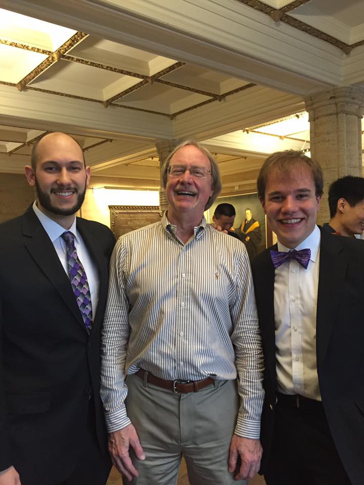
    From left to right: My lab partner Andrew, Professor Frey, and me, Dan

    So what does one have to accomplish in order to get a raspberry pi to become a spectrum analyzer? The real challenge of the project is getting the Raspberry Pi to sample very quickly and reliably, and to perform an FFT on that information. Sampling at a high speed on the raspberry pi was our greatest challenge, but not one we were not able to solve.

    Andrew and I both had a decent grasp on Signal Analysis and the math behind it, so we went to the drawing board to see if we could come up with any ideas to "cheat" the system. Cheating for us would mean analyzing spectra beyond the Nyquist sampling limit. But more on that in the next post.

    In the mean time we had to figure out what exactly we wanted to accomplish with this spectrum analyzer. Sure, it would be awesome to make a spectrum analyzer for a few hundred dollars that could capture signals in the gigahertz or terahertz range, but it is probably not attainable for us, especially since neither of us have done any high speed circuit design.

    Instead we decided to focus on a smaller frequency range. We supposed that sampling at a gigahertz would be a good goal to shoot for. Now before you point out in the comments that a spectrum analyzer that only captures up to 500KHz is worthless, let me try to defend this frequency band.

    From my experience at Lehigh, most undergraduates do not deal with analog signals beyond 500KHz in the lab. And while I am positive others will come up with exceptions, my point is signals under 500KHz are heavily used in education. There's a lot to do in that space, and much of what students are doing is under that frequency threshold. Giving students the ability to not only use an oscilloscope, but also getting their hands on a spectrum analyzer is hugely beneficial. It will give them one more instrument to get familiar with, and also help in signals courses by giving them hands on experience with the frequency domain.

    So now that we have the frequency nailed down, we came up with a few more goals for our project. We wanted it to simply plug into a normal outlet, no fancy extra power supply required. We wanted it to be standalone, so it was going to require its own screen and inputting devices. We wanted simple probes so one could easily hook this up to their circuits and see the results. Finally, we wanted a simple GUI that allowed the user to start capturing spectra quickly and easily, and also have the ability to save spectra and perform more analysis with the raw data.

    That's all for this log. Look forward in the next post to us laying out a system block diagram or two, and describing our superheterodying technique!

View all 9 project logs

Enjoy this project?

Share

Discussions

Similar Projects

Does this project spark your interest?

Become a member to follow this project and never miss any updates