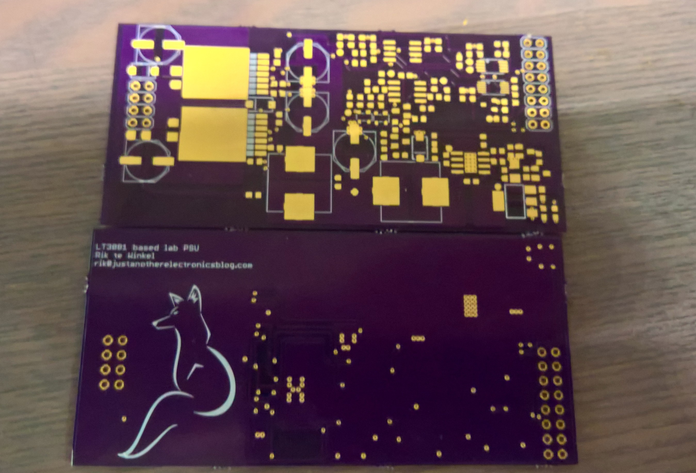
The new board:

Based on the older version of the VederPSU a new schematic was made, using the same DAC and ADC from the old VederPSU but with a different power stage based on the LT3081 app note. The reason for using the same ADC and DAC (the MAX11613 and MAX5802) is that these are one of the very few ADC's and DACs with an I2C interface and a separate voltage reference input. I want a single voltage reference for the whole system to make calibration easier and to be able to pick a voltage reference of choice.
The DAC has 2 outputs, one for the voltage and one for the current. With the current voltage reference they can go from 0 to 4.096V. The voltage output is multiplied by 10 using an opamp to create a 0-40V signal to control the output voltage with. The 0-4.096V for the current is converted to 0-200uA using an opamp. This combined with a current mirror controls the current limit of the LT3081's.
The ADC has 4 inputs, from which one is used as a voltage reference input. The 3 left are used to measure the output voltage, the output current and the temperature of the LT3081's.
The schematics can be found on the project page for anyone who wants to take a look.
Discussions
Become a Hackaday.io Member
Create an account to leave a comment. Already have an account? Log In.