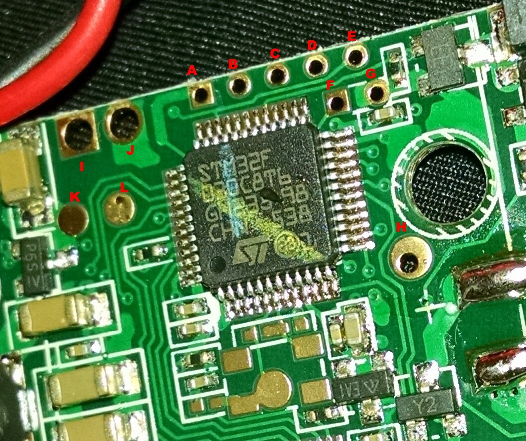
Using this pad reference picture:

E = PA13, D=PA14: SWDIO & SWCLK, as mentioned before. C = NRST. B = GND. A = VDD.
I = VBAT. J = GND. K = VBAT. L = GND. H = ADC1_IN (Probably) as described in a previous log.
The I2C lines are where I might try next.
 Simon Merrett
Discussions
Become a Hackaday.io Member
Create an account to leave a comment. Already have an account? Log In.