 agp.cooper
Understanding Weird CPU
Now that I have spent some time reviewing other CPU project (it is good that I am not the only mad person out there!), I do find it hard to follow their concepts.
So I will try and breakdown my schematic (divide and conquer!).
Before we begin
One instruction - Move
Basically the instruction is:
Move [PC] -> [PC+1]
The CPU moves the data at the address pointed to by PC to the address pointed to by PC+1. So its a just a fetch and a deposit.
Confused?
Answer the question, how would to move data at one memory location directly to another memory location?
Instructions are memory locations
The memory address for the ALU registers P and register Q are 0xF8 and 0xF9, respectively, but:
- If you read register P (0xF8) you get back "P ADD Q" (not the value you wrote to P).
- If you read register Q (0xF9) you get back "P NAND Q" (not the value you wrote to Q).
By the way, other than SHR (which was an omission) this is a complete set of instructions.
You can software code a P XOR Q in 10 instructions.
Making a jump
To make a jump, write the jump address to the Program Counter (PC) at 0xFF.
The four jump options are:
- 0XFF Jump unconditionally
- 0XFE Jump if carry set for P ADD Q
- 0XFD Jump if P=Q
- 0XFC Jump if P>Q
Accessing the front panel
- The address of the Address IO (the bottom row on the front panel) is 0xFA.
- The address of the Data IO (the top row) on the front panel is 0xFA.
- One trick, the input is inverted (and momentary).
DONE!
The Schematic
The schematic has 28 chips excluding the PROM, RAM,and associated memory address decoder.
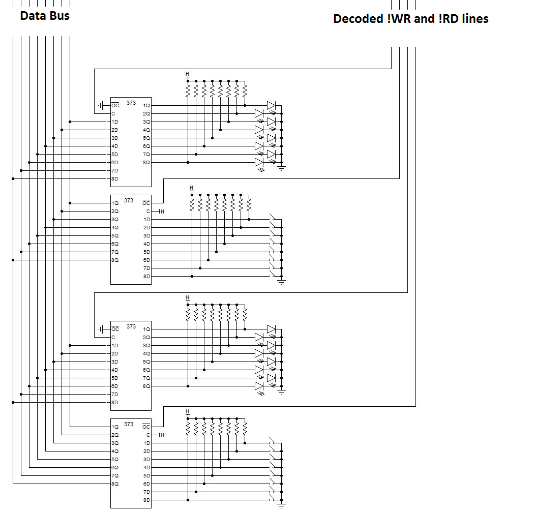
Lets kill off the Data IO and Address IO
Nothing complicated, just basic input and output (IO) - 24 chips to go:
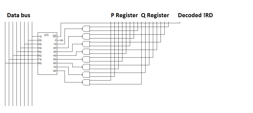
Let kill off the ALU NAND sub-system
Note the ALU sub-systems have common P and Q registers - 21 chips to go:
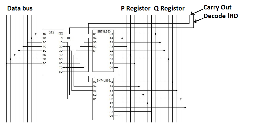
Let kill off the ALU ADD sub-system
Nothing complicated here just two 4 bit adders - 18 chips to go:
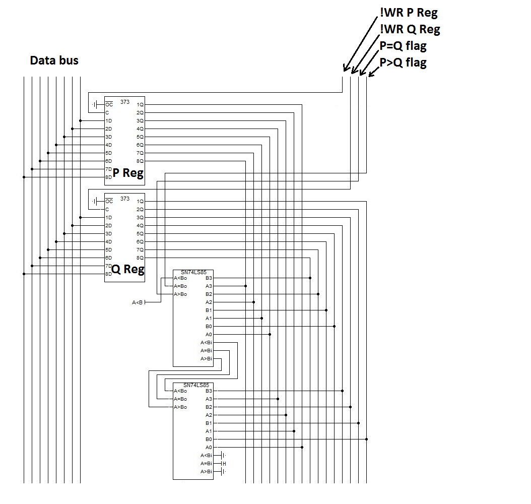
Let kill off the ALU Comparator sub-system
Now we can see the P and Q registers referenced above - 14 chips to go:
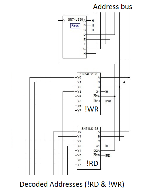
Lets kill off the Address Decoder for the ALU and IO
The decoded address space is 0xF8 to 0xFF but not all are used. Two signal come from the Timing sub-System: !RD and !WR - 11 chips to go:
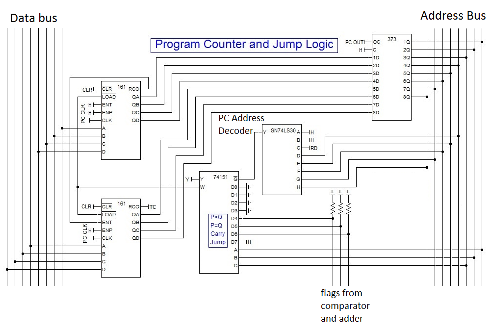
Lets kill off the Program Counter (PC)
This one is a little more complicated as it includes decoding and jump logic. There are a number of inputs from the Timing sub-system (i.e. !CLR, PC_CLK and !PC_OUT) - 6 chips to go:
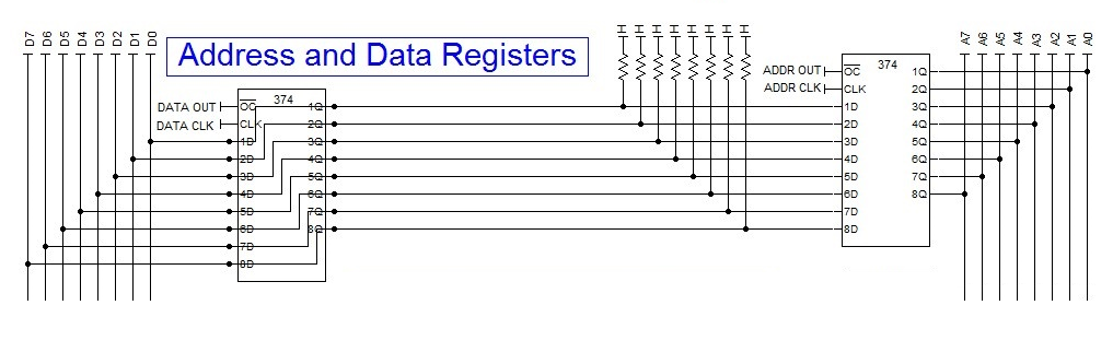
Lets kill off the Fetch and Deposit registers
These two registers (Address and Data) hold the fetch and deposit address (in turn) and the data moved between the fetch and deposit addresses. The PC controls the buses 50% of the time and these registers control the buses the remaining 50% of the time.
The inputs from the Timing System are DATA_CLK, !DATA_OUT, ADDR_CLK and ADDR_OUT - only 4 chips to go:
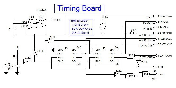
Finally lets kill off the Timing sub-system
What you see here is:
- A clock using a 2 input NAND gate (74LS132). Note that it has been presented as two 74LS14 schmitt triggers and an OR gate. This was necessary because the simulator model for 74LS132 is not actually a schmitt trigger?!
- Reset logic using a 74LS14.
- A two phase clock (74LS93).
- Some timing signal decoding logic.
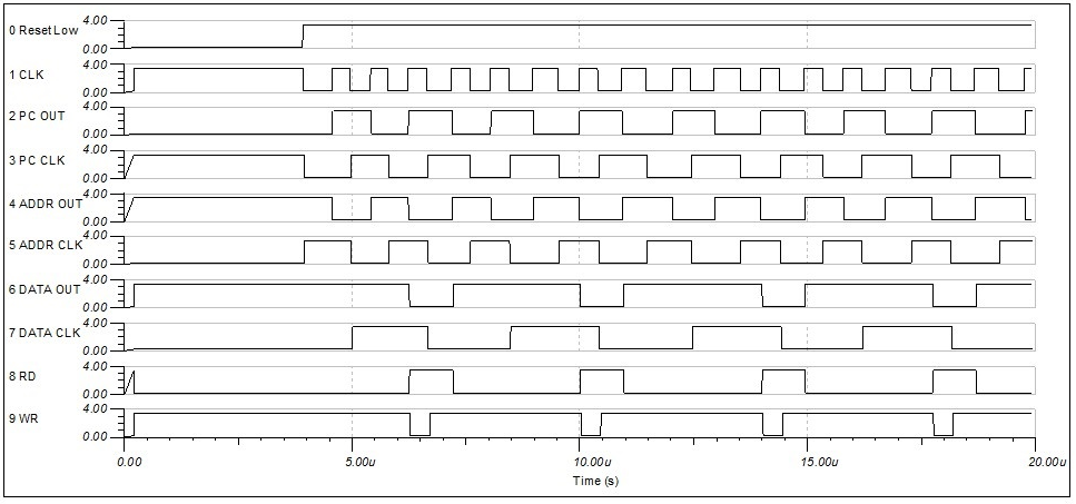
Here is the timing signals from the timing sub-system, it might make more sense now:
Well, you may not get it all the first time but everything is there for you to understand the Weird CPU.
For my actual build, I did not include the comparator sub-section as Jump On Carry is sufficient for a minimal system.
Weird CPU II has some improvements: 16 bit rather than 8 bit, rearranged instruction addresses and the inclusion of the missing SHR instruction. I have also inverted the jump flags (i.e. Jump on not carry, Jump on P!=Q and Jump on P<=Q).
Your challenge, if you accept it, is to design and build your own minimal CPU with:
- a lower chip count, and
- more instructions.
Best of luck, AlanX
Discussions
Become a Hackaday.io Member
Create an account to leave a comment. Already have an account? Log In.