A few years ago, I did a small job for someone on reddit.com, designing a PCB with six buttons connected to a spark core footprint. The person who I was doing the favor for later sent me a spare board that I never ended up using, but sort of hung on my wall like art.
This lead me to realize that there are plenty of hackers who have stacks or stashes of faulty/unused PCBs, most of which will never be used. A well designed, well made PCB is like art: a complex canvas filled with maze-like traces and speckled with vias. In my opinion, every PCB is beautiful, and should be shared with the world.
So, I created this project with the goal of collecting everyone else's spare boards, taking pictures of them, and putting this collection on the internet for all to see. In the process, I am to elevate the practice of electronics CAD to a high art.
Interesting! I was planning to use a white background with some careful lighting to document the PCBs, but it makes sense to use a scanner to get a high resolution, quality picture. I'll have to dig out my old scanner and windows XP box and give it a try.
CCD scanners are still made; it's just most of the cheaper ones that are CIS-based. I saw something recently about this—I think it might have been related to that bury-a-scanner-in-the-ground-to-image-underground-activity project posted on the blog not long ago.
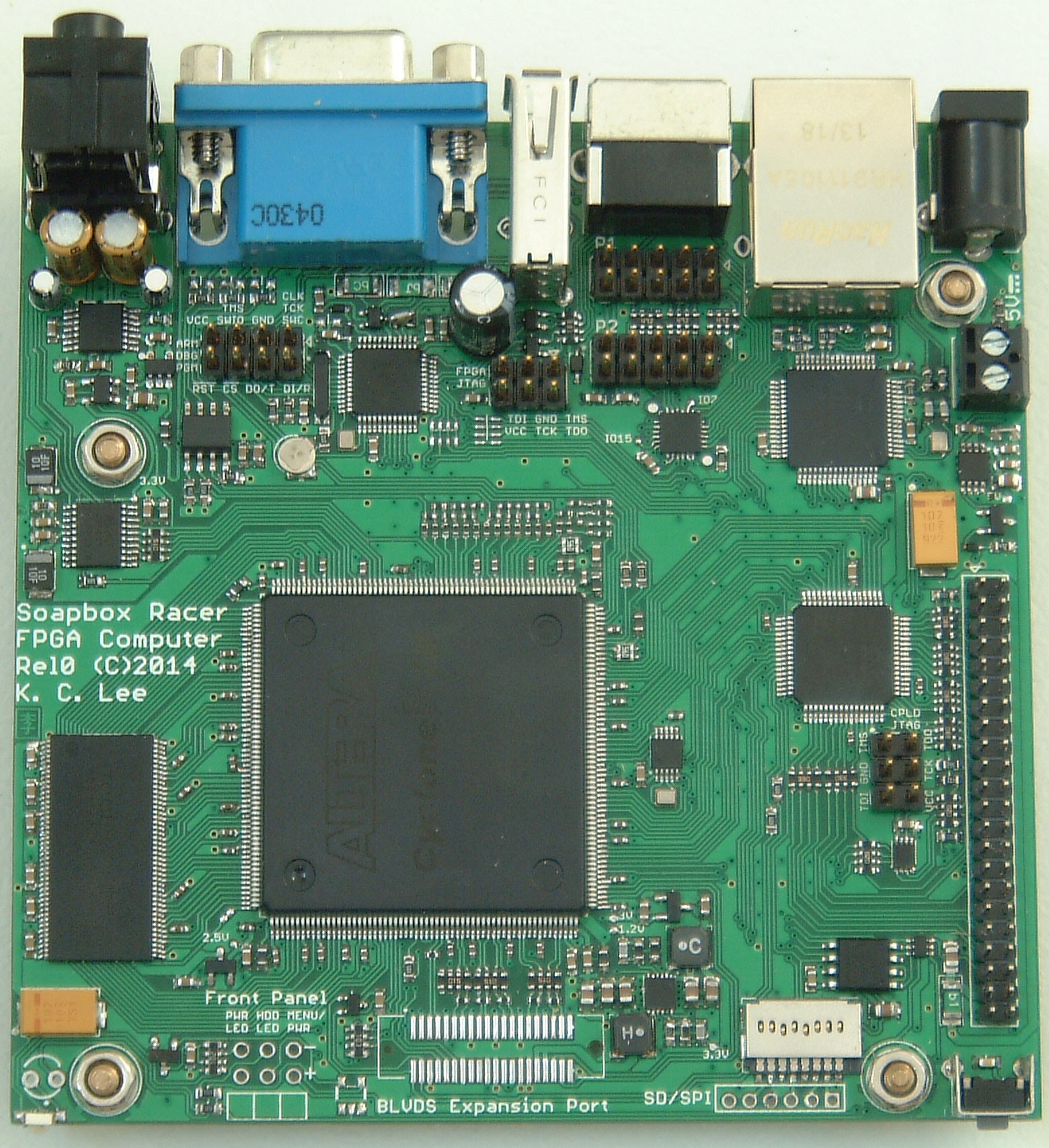
https://hackaday.io/project/1347-fpga-computereval-board/log/6562-blank-pcb-scans-large-files