 Mark Bradshaw
This machine uses a 4-wire incremental rotary encoder instead of the often seen 2-wire encoder. There are 2 signal wires (A, B) and 2 inverted signal wires (not A, not B) in addition there are Z and not-Z signal that are not used. So to read the encoder position I could simply not use the inverted signals and be done with it, but the machine is noisy and vibrates so the additional noise rejection could be helpful. If the engineers at Instron thought it was important then I'm not going to question them. So I thought it would be interesting how they used these additional two inverted signals.I followed the encoder signal traces from where they enter the main board and found they all end up at two chips, U33 and U34, which are both MB14011B quad 2-input NAND gates. Following the other traces showed a circuit with the following configuration:
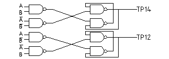
NAND is a logical operator meaning not(X and Y) and is represented by the blocks with a round side with the circle on it. NAND has the following truth table:
| A | B | NAND( A, B ) |
| 0 | 0 | 1 |
| 0 | 1 | 1 |
| 1 | 0 | 1 |
| 1 | 1 | 0 |
If you continue to follow the logic of the circuit you will find that the two pairs of NAND gates of the right side of this circuit have some interesting behavior in that in certain cases the output depends on what the previous output was. This circuit is known as a SR NAND latch and you can find more information about it on wikipedia here: SR NAND Latch.
This circuit takes the 4 encoder signals as inputs and produces 2 outputs accessible at test points TP12 and TP14. Looking at the logic of the complete circuit reveals the nature of the signals at TP12 and TP14.
For simplicity I have assumed that not(A) and not(B) are always correct so no noise.
| Clockwise | Continuous | |||||
| Phase | A | B | TP14 | TP12 | TP14 | TP12 |
| 1 | 0 | 0 | 0 | No Change | 0 | 1 |
| 2 | 0 | 1 | No Change | 0 | 0 | 0 |
| 3 | 1 | 1 | 1 | No Change | 1 | 0 |
| 4 | 1 | 0 | No Change | 1 | 1 | 1 |
| CCW | Continuous | |||||
| Phase | A | B | TP14 | TP12 | TP14 | TP12 |
| 1 | 1 | 0 | No Change | 1 | 0 | 1 |
| 2 | 1 | 1 | 1 | No Change | 1 | 1 |
| 3 | 0 | 1 | No Change | 0 | 1 | 0 |
| 4 | 0 | 0 | 0 | No Change | 0 | 0 |
The output of the circuit is simply the normal 2-wire encoder output however it will not register most cases where one signal changes but it's inverted pair does not. I can use leads to TP12 and TP14 as if they were normal encoder outputs.
Discussions
Become a Hackaday.io Member
Create an account to leave a comment. Already have an account? Log In.