 Pamungkas Sumasta
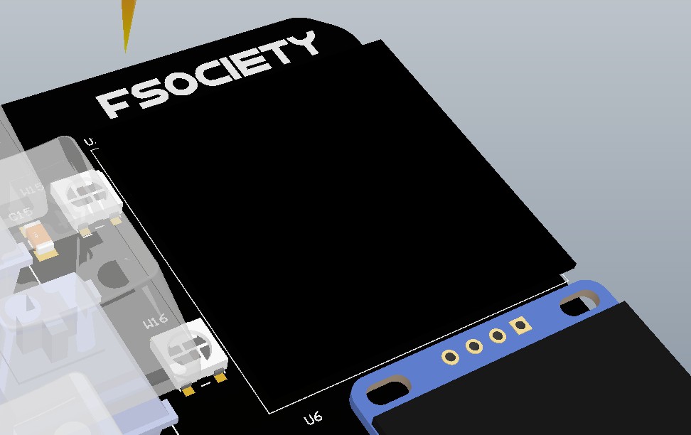
You've probably have enough with the schematic layout in the previous log. It is now the time for the more interesting stuff; The board layout. I've spent the whole weekend to finish this design from making the library, schematic and then lastly layout. Of course, didn't have time to do grocery or even shower during that weekend ;) Even with the rush, I've noticed that I made only one mistake. I swap the VCC and GND in the OLED library. oops. Apart from that is hunky-dory. Below just a preview of the final board design before I explain in more detail about the design choice etc.
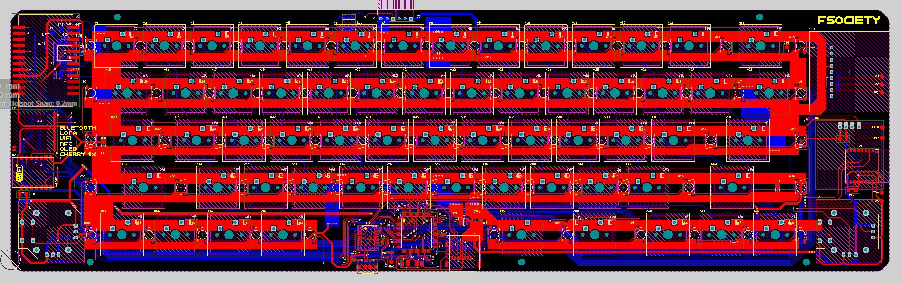
Board Dimension
This was very important in the beginning. I started in the beginning by placing all the cherry mx switch in place with 2mm distance between its widest part. I figured that 300 mm in length should fit all the cherry mx keycaps, but that still excluding other components. all the modules can be placed on the bottom side, but the Joysticks are not possible. it just has to be on the top. like it or not, adding around 33 mm on each side should suffice the space requirements. Initially I was planning to round the length to 400 mm just to make it easy and have some room space for some improvisation later on, but the cost for the PCB compare to 368 mm is significantly quite high. Therefore I stick with 368 mm.
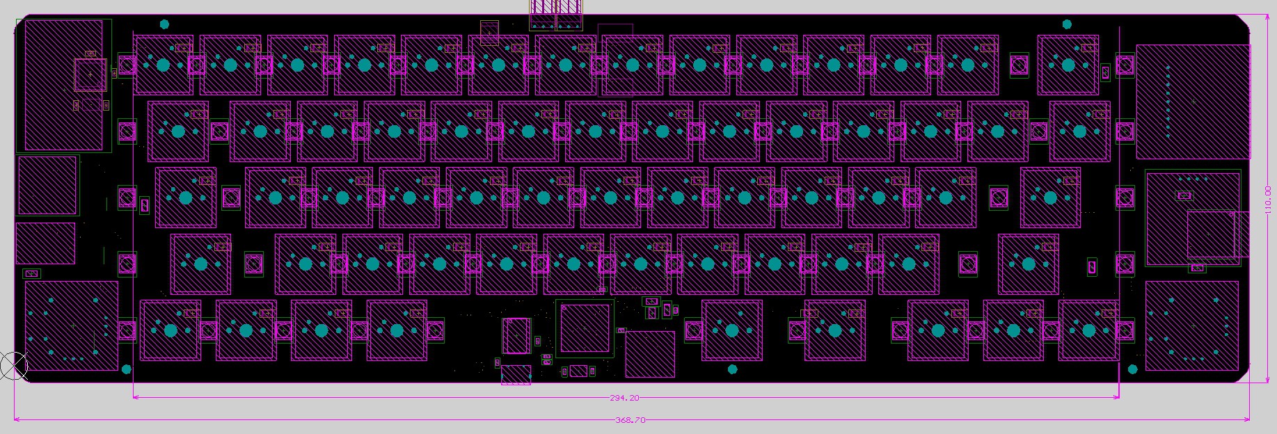
Next thing is about the width, 100 mm sounds like a good round numbers right? Well not really it is only later you realize that you will need some extra width for the array of traces on the bottom side of the board. I decided to add 10 mm to the board width. And needless to say, aesthetically, with 100 mm width, and the tall keycaps, the board looks a bit clumsy. Having some spare width tremendously help the visual side of it. trust me.
Placement & Routing Concept
As I mentioned in earlier Log. I just don't like asymmetry. So since the beginning, I always stay conscious to spread the components evenly. It concludes to several points listed below:
- The main Microcontroller unit is located in the center of the board. not on either side. It is very importat for the sake of the routing. And if you want to stick with 2-layer board as well. I just simply cannot think that it is possible to route the board with 2-layer if you locate the primary Atmega on either side. The routing of the matrix of the switches will easily become a nightmare.
- The primary keyboard is centralized. It has to be the center and the main attention of the board. Unlike most keyboard, the keypad on the right ruins the potential symmetry of a keyboard as a whole.
- One joystick on each side. Instead of having two on the right side for Arrow as well as the mouse. One has to be on the left side and another one on the right side.
- NFC/RFID Reader has to be on the right side. Well yes, because I wear the right on my right hand ;)
- The rest of the modules evenly scattered on the right and left side of the board. And only on the top side. And of course, watch out the cross-talk or some black magic voodoo happening between the antennas. (Need RF guy here to comment)
- WS2812b placed between the Cherry MX switch and the co processor has to be placed on the bottom side. it was simply because there was no room on the top side anymore.
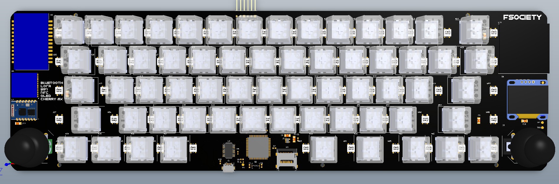
Now that We have the concepts nicely described on a bullet points above. I give you a tour through the design in 3-Dimension concept. Needless to say, this is one of the perks in using Altium.
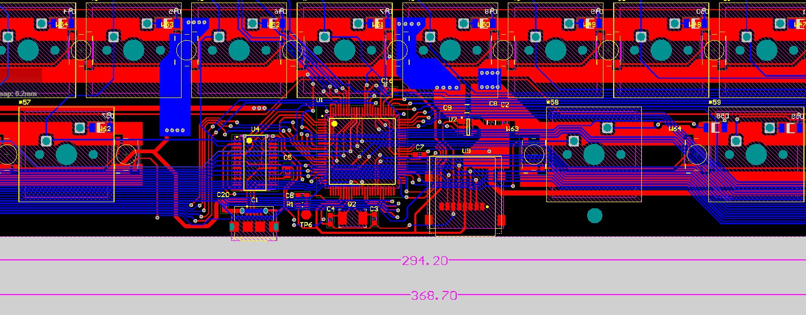
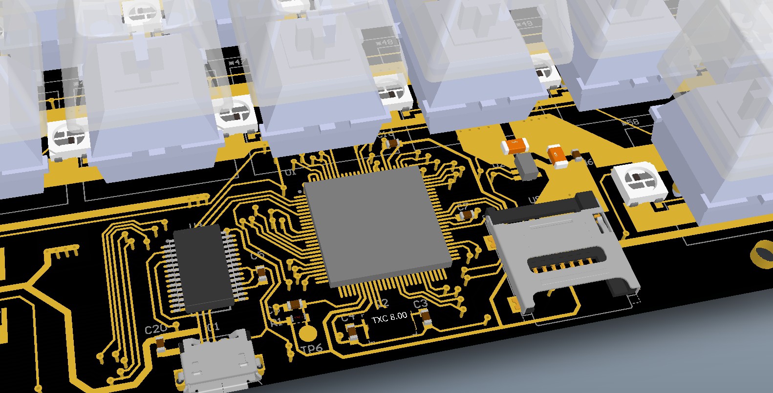
Main Microcontroller ATMEGA2560
The microcontroller as you see above is located in the bottom center of the PCB. hiding safely in underneath the space button. (FYI I didn't have a step file of any other keycaps except the standard one). It was quite a fortunate thing to have such a empty space just on the spot where I needed. If you lok at the picture below, all the Row and columns from the key matrix can be routed easily. Making it more like a star topology. Don't forget it is not just for the sake of routing the switch matrix, but also all other peripherals on either side of the board. On the second picture below you can see all the communication bus propagates to either side equally. I strongly believe this was a good design choice. Moreover, the USB connector you see below is for programming and debugging purpose.
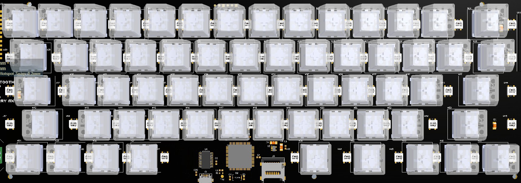
 The Switches array & the LED
There are 62 Cherry MX on-board that are surrounded by 68 WS2812b RGB Led. The final result shows as follow:
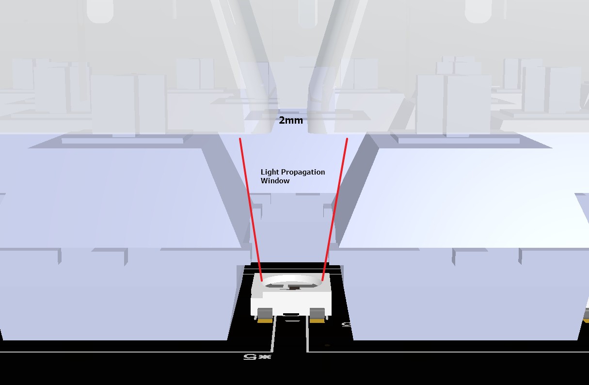
The challenge was quite simple but was a bit tricky as well. I had to find just enough spacing between the keycaps that is not too big and not too small allowing the Light from WS2812b to pass through while not sacrificing the typing ergonomic. Also at that time, I just haven't got a clue what was the tolerant of the Chinese transparent keycap. Having it too narrow posses quite some risks. Moreover I simply couldn't get the best out of the ideal light propagation angle from the WS2812b for typing-ergonomic.
However, following some prototype printed on a piece of paper, it seems that 2mm clearance between the keycap will be good enough. It will still be comfortable for typing yet also the light propagation windows doesn't get too narrow. In the future, I will definitely use the family series of Cherry mx switch that has transparent housing instead of the boring-black.
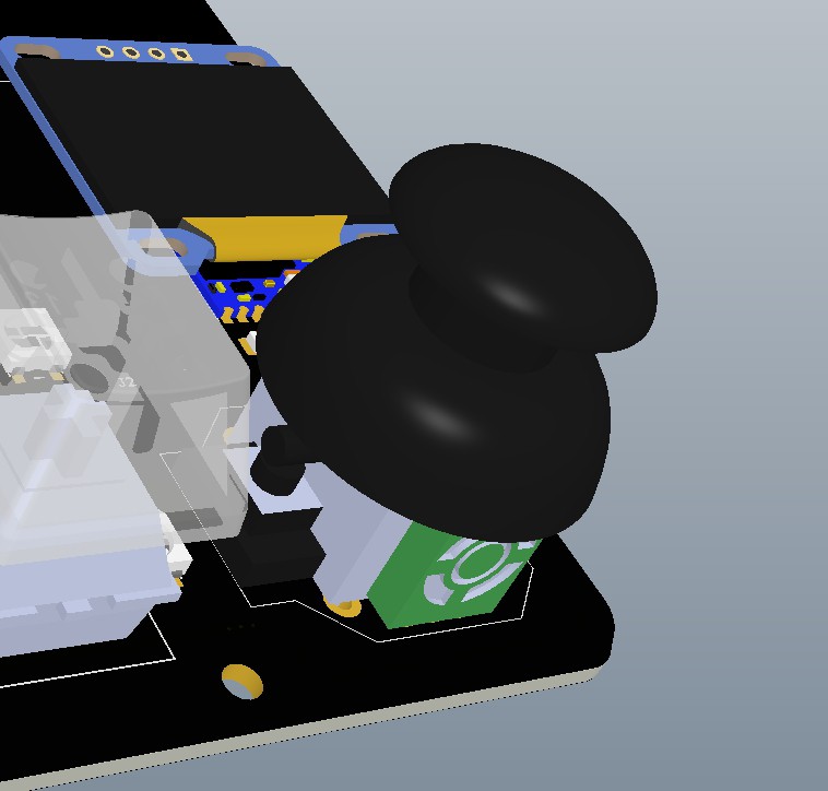
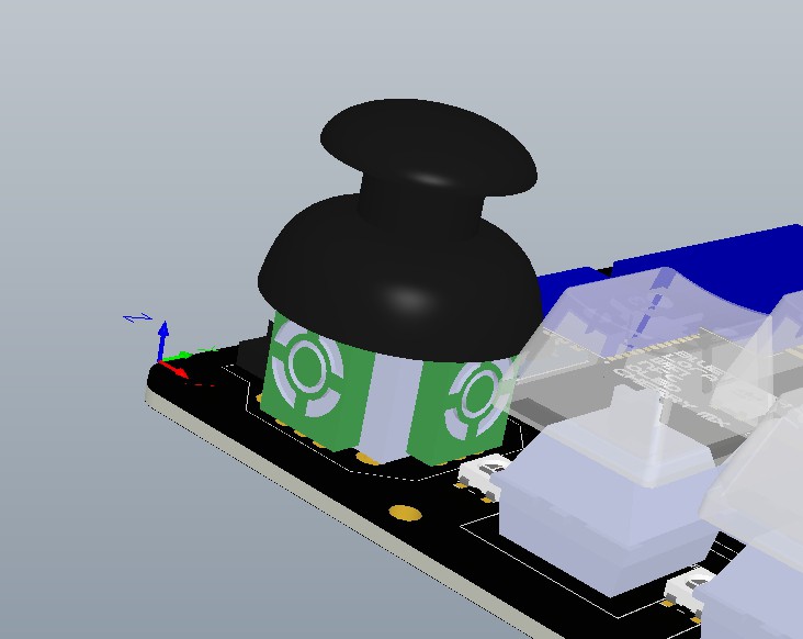
 One Thumb Joystick on each side
Yup. I don't think that is bad idea after all. I could've put both joystick on the right side because I'm right handed. But then I won't have space for the NFC tag on the right side. So having in on either side sounds like the best options. The right one for arrow buttons while the left one is for the mouse movement.
NFC/RFID Reader on the Right hand side
For obvious reason, I use NFC ring on my right hand fingers, so obviously no question where I should place it. Interestingly enough this particular module has antenna that is on the other side of the primary component side. So once mounted on the primary keyboard, you only see the logo of the antenna and that's it.
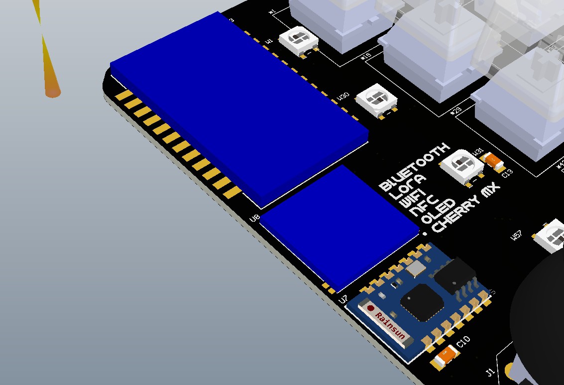
The rest of the Modules
Started from the right hand side. There are two more modules that hasn't been covered yet. And those are the OLED and the Bluetooth 4.0. The tiny bluetooth module hid underneath the mini OLED display as depicted on the picture below. So far it didn't quite give any performance issue regarding the wireless transmission etc. 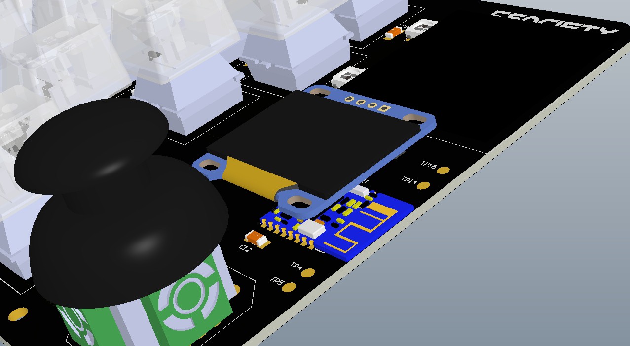 Moving on to the left side. There are three modules that is placed next to each other as can be seen on the picture below. The biggest blue rectangle on the top is the Bluefruit HID (couldn't find a .STEP file for it unfortunately) while the blue in the middle is the LORA module, and the lowest one as you'd probably have known is the ESP8266 module. Bluefruit HID and the ESP8266 Wifi module talks in 2.4Ghz while the LORA is sub 1Ghz. Haven't test much the transmission performance of the antenna up to this point. However, the Bluefruit HID and the ESP8266 seems to work just fine.
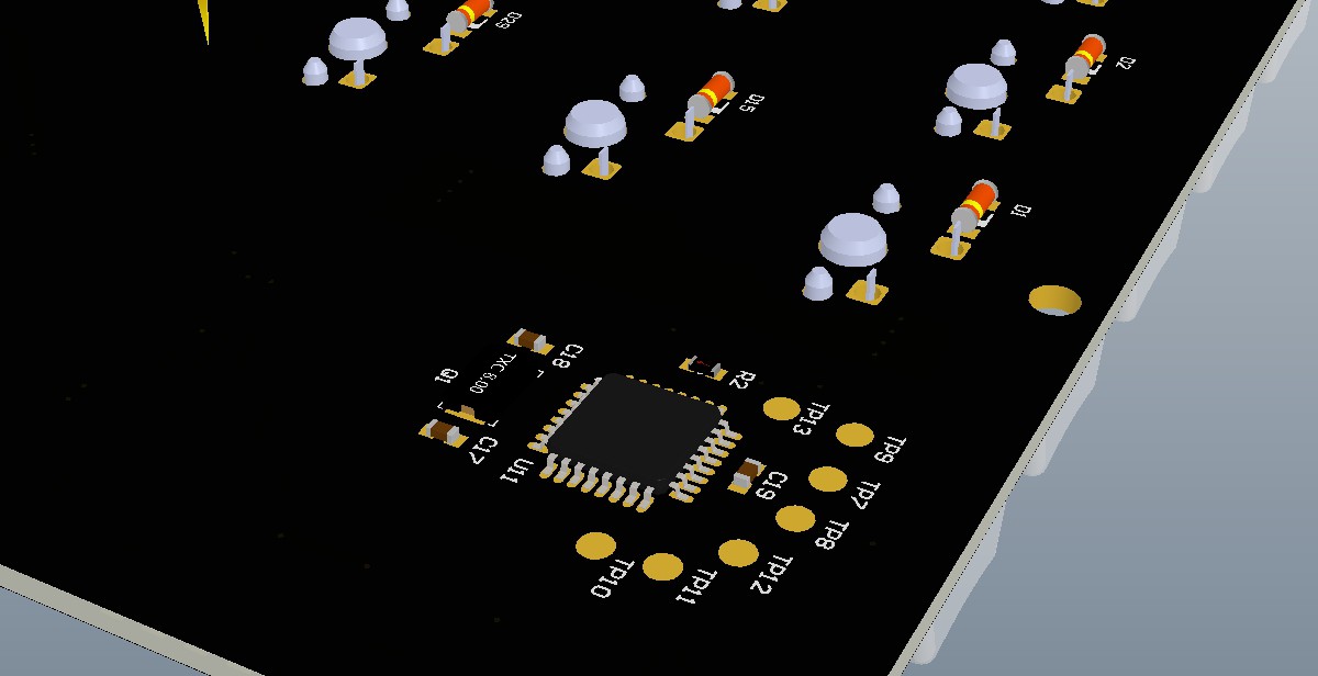
 The Co-processor aka the LED Driver
There isn't much happening on the bottom side quite frankly. Only the dedicated LED driver which is the ATMEGA328p that is located on the bottom. Also diodes that was replaced by resistor in the final assembly.
Well, that was it. You can file on the project documents or here the 3D adobe PDF file of the design. What you need is only a Adobe Acrobat reader ad have fun browsing through the design.
Discussions
Become a Hackaday.io Member
Create an account to leave a comment. Already have an account? Log In.