The goal of Printem is to let anyone easily, quickly and cheaply create Printed Circuit Boards for prototyping use. Imagine if one could create single layer, copper PCBs in less than 2mins after you design them, one will be able to quickly test and iterate on the designs, we believe that Printem is a useful tool for anyone who works with electronics and hardware.
So No Etching ! , No Special Inks !, No Special Equipment ! All you need is the Printem Film and a normal home office printer.
The build logs goes into how an end user would use Printem, this will be followed by posts on how the Printem film works, how to make your own and the current work that is being done on improving its various attributes. We would love to hear your thoughts on how useful Printem might be in your daily work.

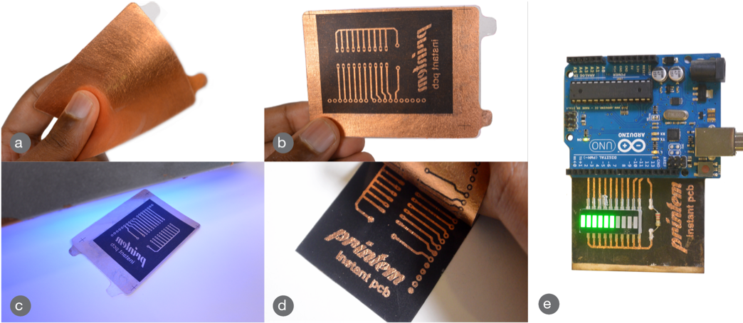
a) The key to Printem is the Printem Film - which i s a multilayer stack of materials that work together to produce the final copper PCB
b) The circuit pattern is printed on the Printem Film using any laser or inkjet printer using black ink
c) The film is then exposed to UV light or sunlight for 30 seconds ( or lesser if the light is intense )
d) The top layer is peeled off , revealing the copper PCB underneath, this is ready to use
e) This just shows a simple LED bar graph being interfaced with an Arduino.
All this only takes about 2 mins !
 varunperumal
Discussions
Become a Hackaday.io Member
Create an account to leave a comment. Already have an account? Log In.