One of the first things that caught my eye, when I did some preliminary research, is the beginning of the Wikipedia page about ECL's history:
"
Yourke's current switch was a differential amplifier whose input
logic levels were different from the output logic levels. "In current
mode operation, however, the output signal consists of voltage levels
which vary about a reference level different from the input reference
level."[16]
In Yourke's design, the two logic reference levels differed by 3 volts.
Consequently, two complementary versions were used: an NPN version and a
PNP version. The NPN output could drive PNP inputs, and vice versa.
"The disadvantages are that more different power supply voltages are
needed, and both pnp and npn transistors are required."[9]
"
Can you hear my headgears spinning ?
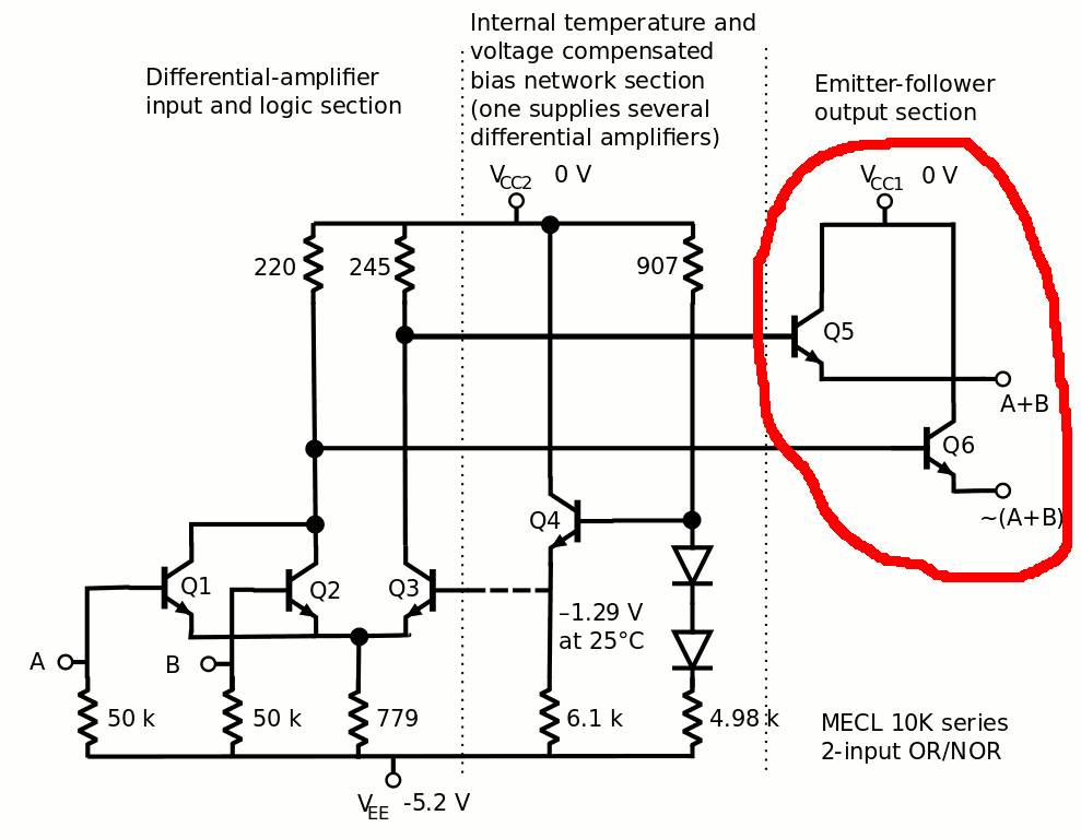
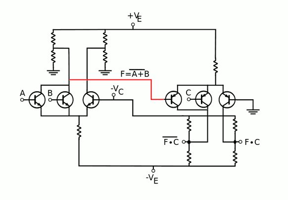
The provided schematic was actually very tempting:
I'm still confused about the reference things but this got me thinking.
Unfortunately, the link to the original paper is down and I can't get the PDF.
E. J. Rymaszewski; et al. (1981). "Semiconductor Logic Technology in IBM" (PDF). IBM Journal of Research and Development. 25 (5): 607–608. doi:10.1147/rd.255.0603. ISSN 0018-8646. Retrieved August 27, 2007.
But there is a very good reason to use this alternating method : save on the output/buffer/emitter follower transistor (when the fanout is 1 or 2).

For the Germanium version, I only have PNP types. NPN are too rare and out of price for this idea so I'll stick to the classic version.
But I'm planning a Silicon version and guess what ? PNP and NPN are about the same price !
The complementary ECL idea is why I got a bunch of BC549C and BC559C : not as fast and shiny as the AF240 but dirt cheap and flexible. Rated at 250MHz "only", they have a much better amplification that compensates and makes them more efficient as general-purpose switchers. They would probably consume less current (save power) and require less buffers.
Now there is a little problem : for the alternance to work, there must be an even number of "stages" to pass through. Fortunately,
- the "buffer" can be used to skip an alternance
- there are circuits that naturally fit !
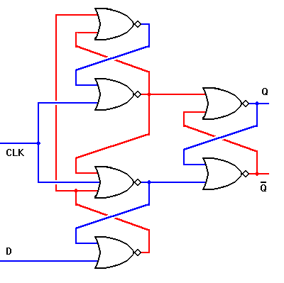
One good example of 2) is the DFF gate as described at http://www.play-hookey.com/digital/alt_flip_flops/d_nor_flip-flop.html
 (thanks to @Ted Yapo for the link at https://hackaday.io/project/11677-the-diode-clock/log/37976-ddl01-hex-nor-gate )
Do you see those red and blue lines ? Well they can be reorganised a bit but everything is here !
The blue lines can come from NPN gates and the red lines from PNP gates. With one exception (the clock), all the gates go to a complementary gate (PNP to NPN and vice versa). The clock case can be solved by a differential clock signal.
So a one-bit synchronous memory can be designed with 3 PNP gates and 3 NPN gates, each with 3 (or 4) transistors.
I don't think it's a coincidence since I have vague memories about this circuit that I saw long ago and was coming from IBM. The same company that created ECL's ideas...
I write all this here because I haven't yet created a project page for the silicon processor but that's something I'll definitely experiment with !
If the prospect of a 250MHz "only" transistor is worrying, worry not : there are faster transistors (but they are more expensive) and the KSP10 is rated at 650MHz. This will be a welcome speedup for the critical datapath (the adder). And if it's still not enough, the BFR96 is rated at more than 3GHz. Damn, my DDS can only reach 200MHz, I guess I'll have to create oscillators with these very same UHF transistors...
Still there is the old problem of feeding this speed demon with data and my fastest SRAM chips reach only 250MHz (the speed of the Cray-2).
 Yann Guidon / YGDES
Discussions
Become a Hackaday.io Member
Create an account to leave a comment. Already have an account? Log In.
Fyi if you're willing to accept long pipeline delays and coding an FPGA, the IOSERDES modules of the Spartan 6 FPGA will pump data at up to 950mbps per pin or pin-pair with the common -2 speed grade. Note: keeping all the bits and clocks in sync at speeds this high is a challenge that usually requires in circuit tuning of signal delays. (i.e. the IODELAY blocks) Afik, this is why nearly all chips with parallel buss interface top out at 250MHz.
Are you sure? yes | no
I suppose so :-)
I have ProASIC3 FPGA with 700mbps differential pairs...
But the point of this project is to do everything with vintage, discrete parts and rediscover our elders' trade :-)
Are you sure? yes | no