Ran into problems on day 1!
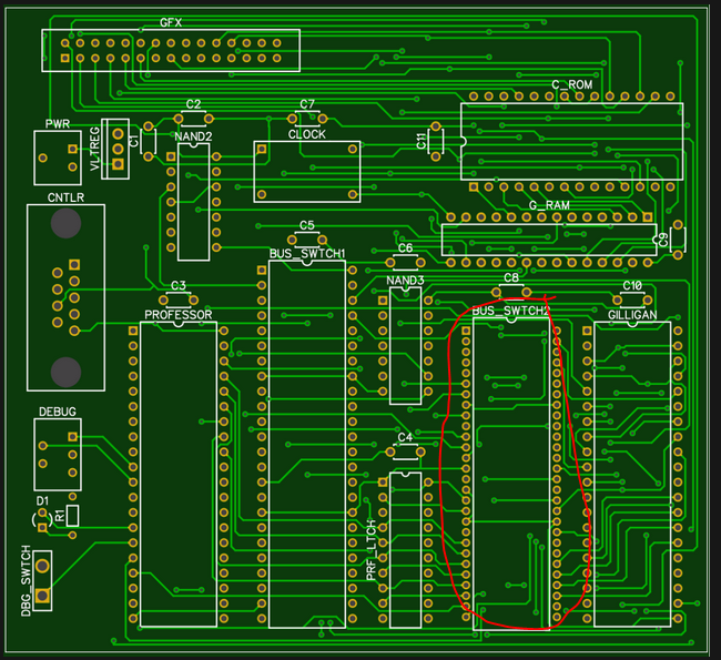
First - I messed up a chip pattern when designing the PCB and the through holes on BUS_SWITCH2 are too close together... It turns out I used DIP-56/600mil/x1.778 - I had no idea what x1.778 meant.. apparently it means the holes are closer together.. I'll have to research that more.
Second - the patterns used for BUS_SWITCH2 and BUS_SWITCH1 were reversed! BUS_SWITCH1 should be a DIP-56 and BUS_SWITCH2 should be the DIP-48.. I'm not sure how that happened, but I'm still learning all the tools with DipTrace, so ... you know.
Third - A couple of the lines failed to route and I didn't catch it - in DipTrace you can go to Verification->Check Net Connectivity to validate everything is routed correctly. Lesson learned!
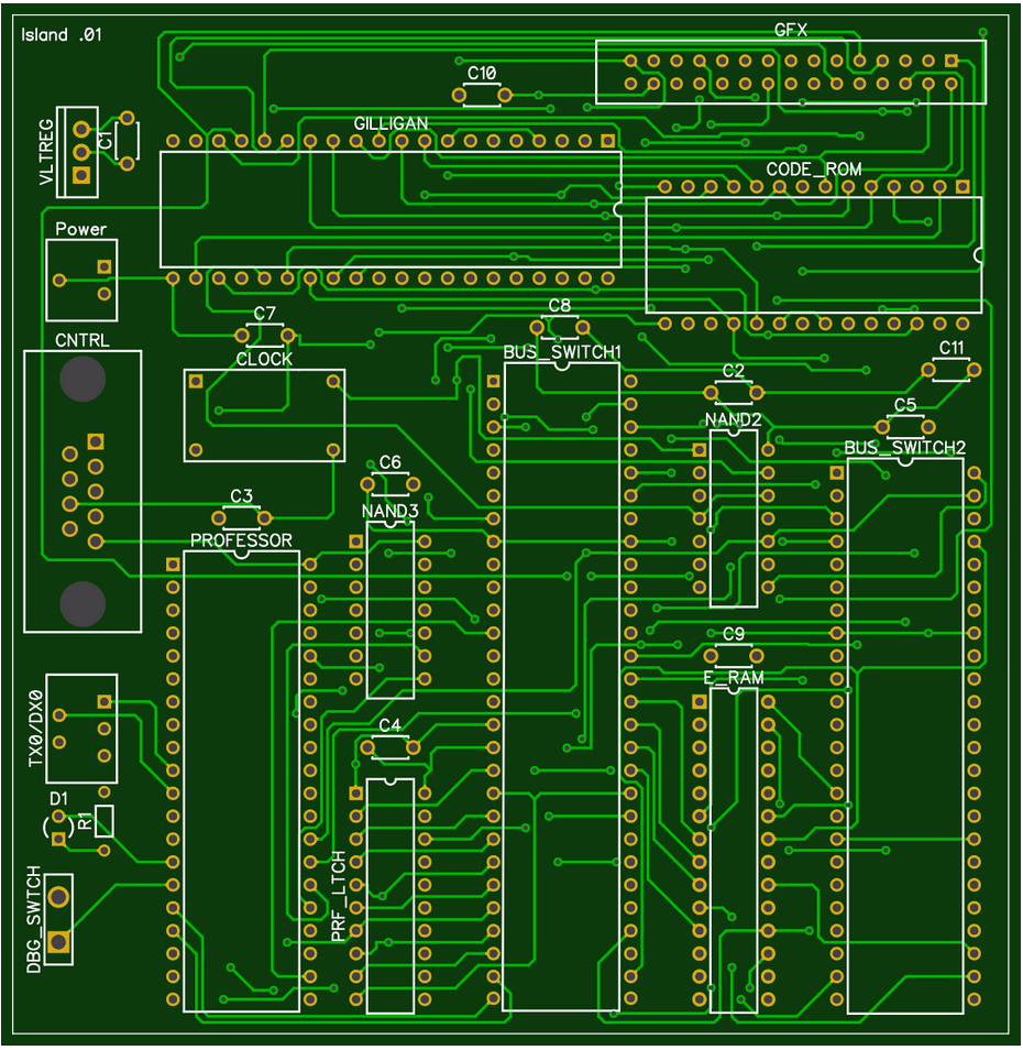
Fourth - I figured I might be doing a few of these with my trial and error - so I started adding versioning to the board.
Here is the previous one - with the red circle around the most egregious error I made:
And here is the new one.. I just ordered it from jlcpcb.com and I'll update when it arrives!
Discussions
Become a Hackaday.io Member
Create an account to leave a comment. Already have an account? Log In.