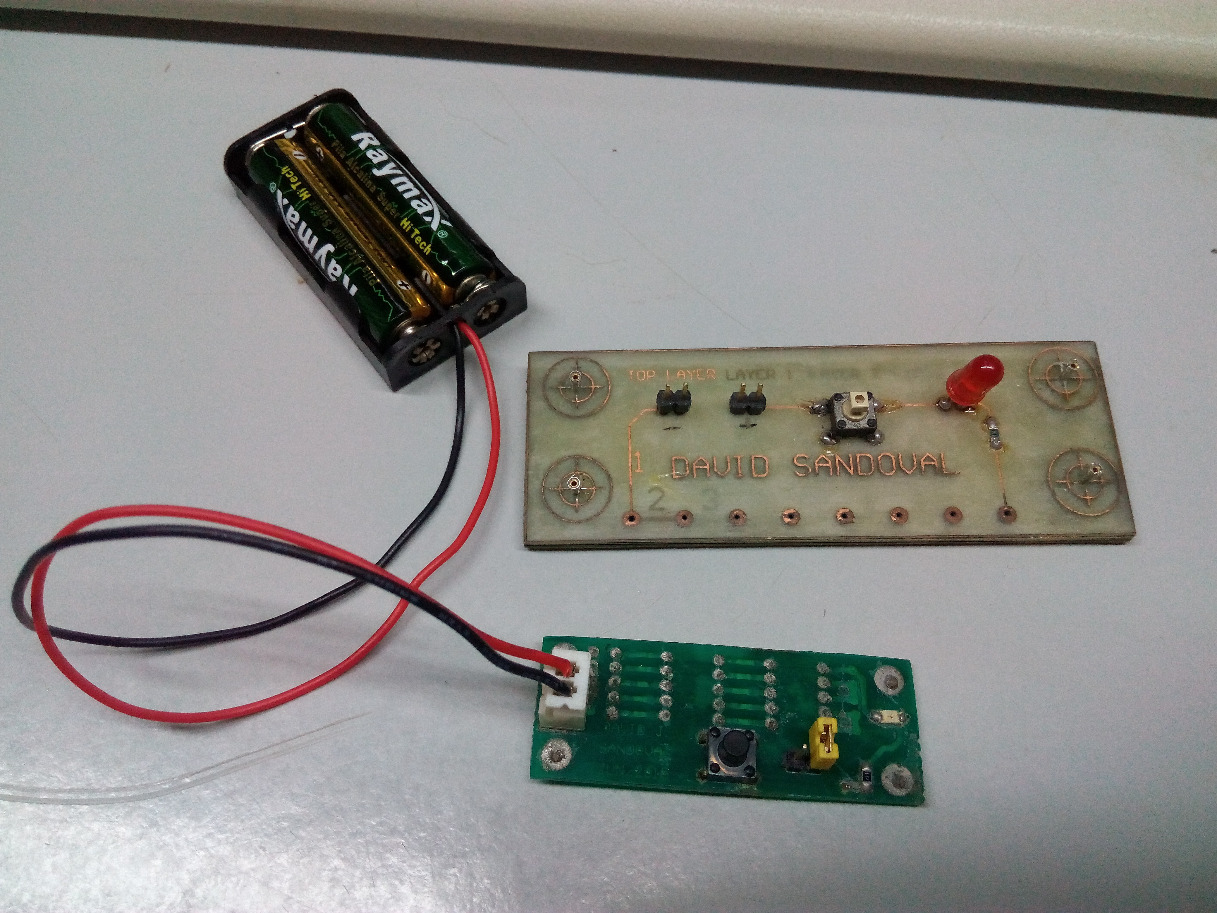
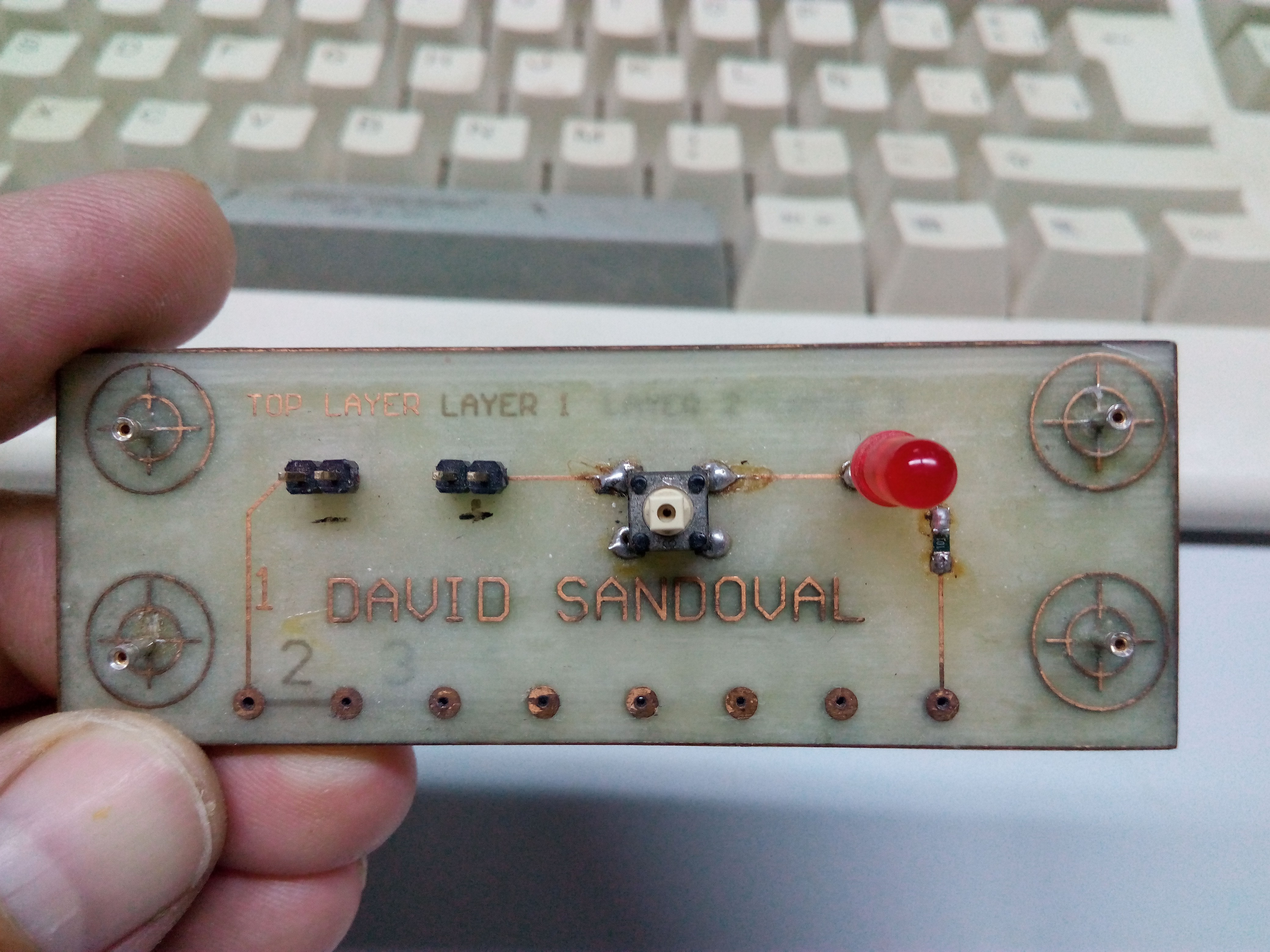
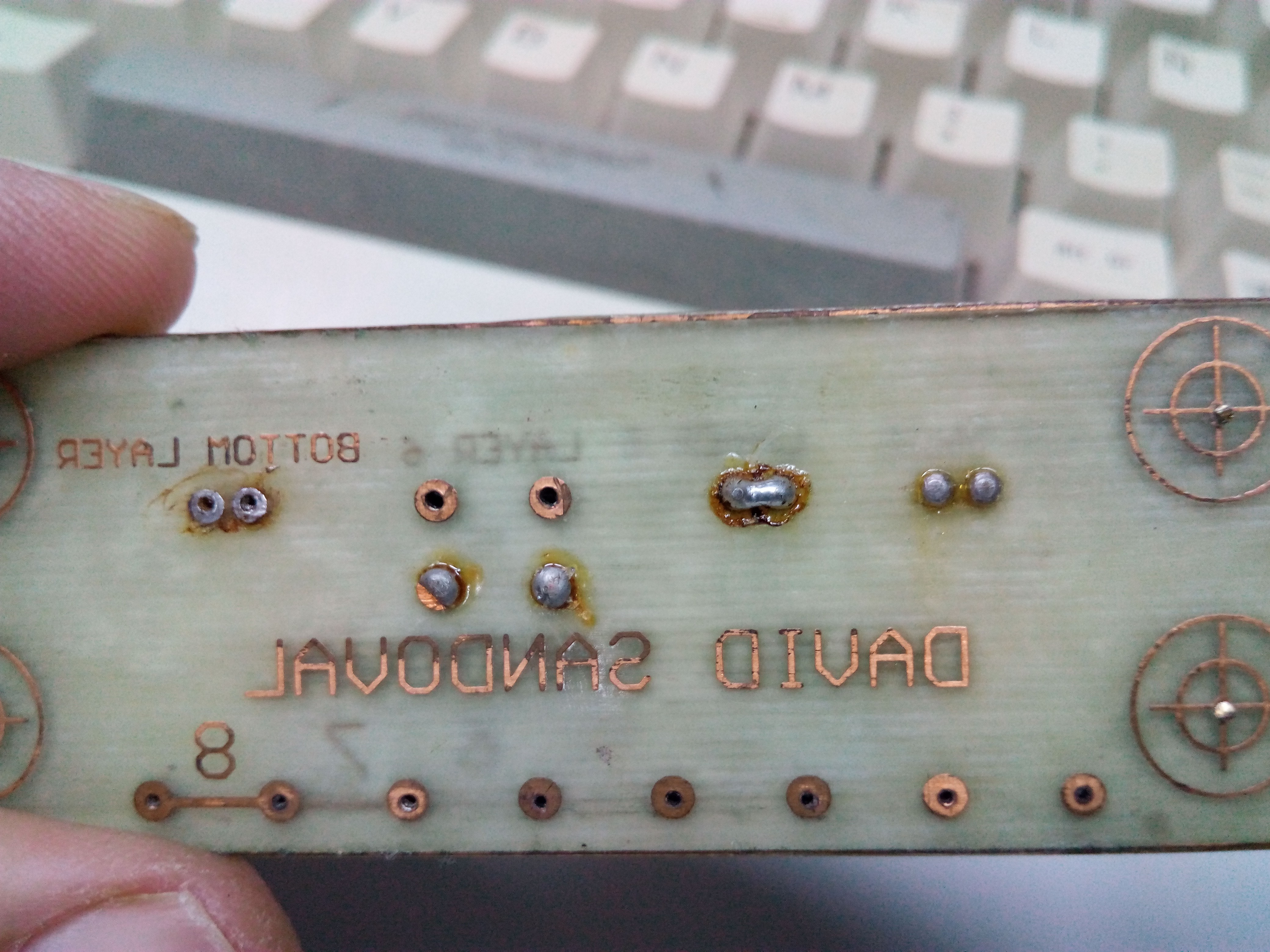
Multilayer PCB (up to 8 layers) with plated-through holes (and vias) at home.
PCBs make prototypes at home, it has indisputable advantages of cost savings and time.
The challenge is to do with the resolution (multilayer) and reliability of entrusting them to an external company.
This problem come by suffering all hackers in each new project.
This project (EBC Bilateral Brain stimulator) equipment for EMDR stood to devote to solve this problem that has taken me over a year.
I can now say that I have been satisfactorily resolved and I can make prototypes up to 8 layers with metallized tracks and drills step.
I show you a simple example at this link


 David J. Sandoval
Discussions
Become a Hackaday.io Member
Create an account to leave a comment. Already have an account? Log In.