Close
0%
0%

Itsy-Chipsy: Make your own $100 chip

Itsy-chipsy is a chip platform that enables a multi-block service like-oshpark capable to offer area for your own chip, for as low as $100.

Similar projects worth following
Raspberry Pi and Arduino have been driving forces to the open hardware community by engaging new generations to hardware engineering. Although board layout and schematic files have been open sourced, the beautiful part of hardware engineering remains hide it inside packaged silicon. Pushing the fences of discrete hardware engineering to the chip engineering field would empower a new tinkerer generation with new applications from the user side.

Not so long ago, access to small-pitch and multi-layer board manufacturing was a privilege for companies. Now we enjoy services like oshpark where by $10 we can get a 1-inch 4-layer board with a ENIG finished. We foresee in the near future several like-oshpark prototyping services for true-cheap chip manufacturing. This project aims to put the first stone by open sourcing a platform for multi-project chips that we called itsy-chipsy.

Chip prototyping used to be prohibitive for small startups and academy until services like MOSIS brought down prices to few thousands dollars per mm2 -in technology nodes capable to run circuitry at moderated performance-. MOSIS runs a multi-project wafer service that aggregates multiple designs onto one mask set to reduce prototyping costs. This aggregation restricts minimum sizing to few millimeters bringing down prices from hundred thousand to few thousand dollars.

However, as an example, five thousand dollars budget for a college in a developing country might be a big number. It is definitely a huge number for a tinkerer or an engineer student ambitious enough to leap from the discrete world to the integrated planet. A service capable to deliver a chip for hundred dollars would break a paradigm and place a bridge to a community always hungry of new chips.

Although getting a chip designed is not as easy as getting a board layout, it might be a reasonable path if you get the required tools and support to get it done. For instance, at most of VLSI graduate programs, making a chip is a tortuous route considering the lack of support and libraries. At grad school, the lack of pads, basic blocks and digital support, make mostly 90% of the work required to prototype your circuit ideas. Having a chip platform where you just can plug your supply nodes, digital calibration data, input and output signals, would bring down chip design from several months to a few weeks.

Itsy-chipsy is a chip platform with the required basic blocks to get a chip done. A platform with onchip regulators, voltage references, current sources, pad library, SPI, JTAG, clock generators, temperature and process monitors. 
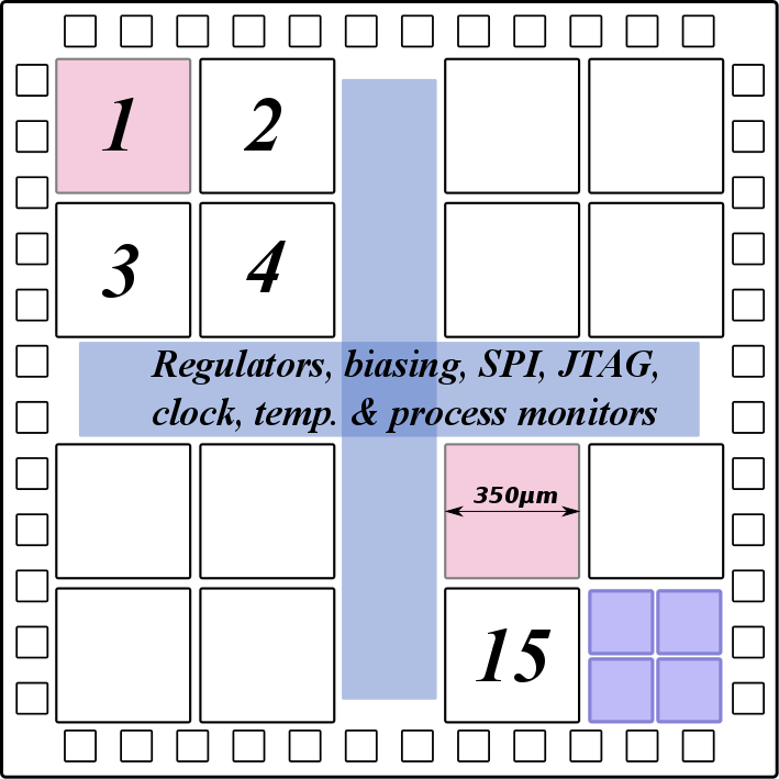
Itsy-chipsy
Utility blocks in a 2mmx2mm chip size

These utility blocks are placed on the chip to service blocks designed by users of the service. With this chip platform, we paved the way to a multi-block service like-oshpark capable to offer silicon area for your own chip, for as low as hundred dollars.

The itsy-chipsy platform has been partially implemented on chips with several blocks:
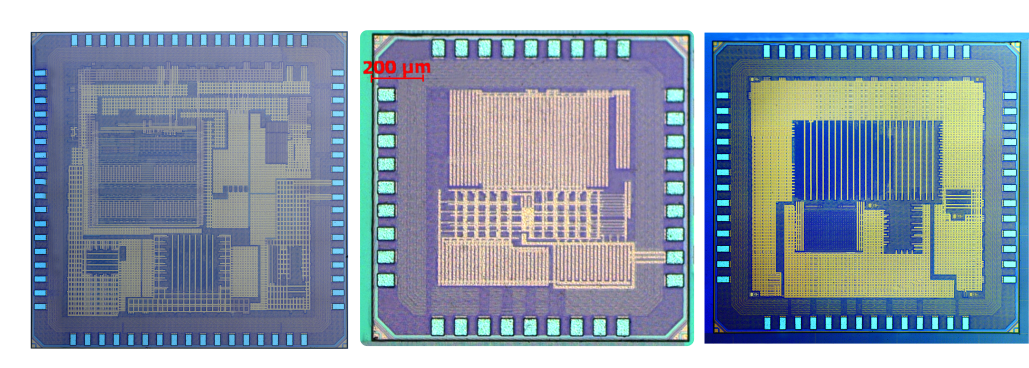
Chips
Chips where some basic blocks from itsy-chipsy platform have been used.

We are working on the second version of the platform and we are expecting by the end of summer, preliminary results should be reported. By September 2018, prototype chips would be available for demos. The second version aims to service a 16 multi-block chip. For instance on a 2mm by 2mm chip in 180nm CMOS technology, 16 blocks of 350umx350um can be instantiated. Where for each 350umx350um block, the fabrication cost will be 350 dollars. Each block will have access to supply pins, SPI, JTAG, regulators, biasing, so the 350umx350um are full real-state for your circuitry. To give some perspective, you might place a basic 32-bit RISC-V-based microprocessor with the basic instruction set on that area. You will have thousands of transistors available for you to get your idea on-a-chip!

A 350umx350um block can be splitted in four, bringing down the price to 100 dollars per a 170umx170um block. A 350umx350um user can get 2 fully packaged chips in DIP 40 pins package or 2 QFN packages with 40 pins 5mmx5mm 0.4mm pitch. A tinker ambitious enough can get her/his own packaged chip for just 100 dolllars!
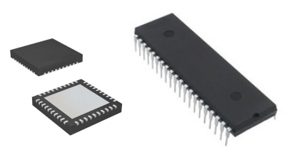
Packages
Packages to be used for the service: QFN 40 5mm 0.4mm pitch and DIP 40 Pins

Couple of foundries are interested and are fully supporting us to get this kind of model ahead. After the platform chip is fully qualified, and current open-source tools are enabled for the technology node, we foresee a crowdfunding campaign for the first oshpark-like chip in 2019.

We are the team behind the open-source 32-bit microcontroller. A chip with the RISC-V instruction set and built-in with peripheral...

Read more »

  • Visiting chip fabs at Hsinchu - Taiwan

    Onchip07/05/2018 at 20:31 8 comments

    We went all the way to Hsinchu at Taiwan and visit couple of fabs and meet with senior directors to discuss the ins and outs of the project. After going to different details and receiving feedback, we agreed, in most cases, that fabs-lawyer departments have to check details to do something similar to what has been proposed. 

    The most difficult part is related to NDA "aggregation". Although MOSIS and Europractice (EP), have something similar, MOSIS and EP customers are big schools and companies with a lawyer office backing them which give confidence to fabs. Let's put a case. Let's assume 16 makers decide to do their own digital chip and each of them pay U$350 to get a chip. Each maker require to sign an NDA with the fab to get access, even, to a minimum info such as digital library files containing fab info. Getting a NDA signed with UMC, TSMC, Powerchip or similar fabs require to fulfill some conditions from the maker side. 

    Although we have had already studied the NDA issue among the outs before visiting fabs, our proposals to solve this issue require full revision from the legal department of the fabs. Brainstorming at the fabs, we believe we have a way to go for the case of digital blocks with a more relaxed NDA. For the analog and mixed signal blocks, there is definitively a longer path and we have to work further details. 

    We are looking and putting details together to get a detailed plan to go ahead and start our fist prototype with 16 participants. Considering that we will publish soon a call for participation, we would love to hear from interested people the following: what digital chip you would do with a 350umx350um area in 180nm technology 9-tracks standard cells library using qflow ? Remember that you will have access to supply pins, SPI port, JTAG port and regulators besides the area given. Please leave us a comment with the description of the circuit and give us some insights of your expertise to show us that you can accomplish a successful run. 

    Apart from technicalities, we were amazed that competitors are all across the street:

    Since the technology war is quite hot, security measures are obviously enforced. We were not able to take a picture even from the parking lot considering security reasons. Even our laptop got cool stickers:

View project log

Enjoy this project?

Share

Discussions

kedharmunigela wrote 06/02/2020 at 09:41 point

we are trying to setup a small scale fab ,how this can help us ?

  Are you sure? yes | no

Nikhil Bajaj wrote 01/09/2020 at 18:33 point

Hi there! Really interested in Itsy Chipsy. Has this progressed any further?

  Are you sure? yes | no

Mikhail Svarichevsky wrote 07/08/2018 at 00:40 point

I suggest to prepare VirtualBox virtual machine running Debian, with all software preconfigured for synthesis and tests, with some very simple design already there (LFSR counter for example) and with some SRAM. This way many would be able to quickly have designs done based on pure Verilog experience. Among all the IP memory is probably the most important.

  Are you sure? yes | no

Mikhail Svarichevsky wrote 07/07/2018 at 21:41 point

Will you power down unused designs? If not - single short to ground could ruin the run, or some error in the design drawing too much current...

How enabled design is selected? Some code via SPI/JTAG?

Could be fun if there is some cryptic 64-bit enable code for each design and it was possible to share it, if author would allow it.

  Are you sure? yes | no

Onchip wrote 07/10/2018 at 14:20 point

We woud have power gating capability for each design. All designs are going to be checked at aggregation for LVS/ERC.

  Are you sure? yes | no

matt venn wrote 05/08/2018 at 08:21 point

I'm interested! Sign me up for the first batch!

  Are you sure? yes | no

Giovanni wrote 05/02/2018 at 21:37 point

Awesome! I believe this is a cornerstone enabling open HW development and sharing!! Can't wait to hear news about this!

  Are you sure? yes | no

cheater wrote 05/01/2018 at 11:45 point

if I want to build much simpler analog chips, will it be possible to fit more than 4 such sections on one chip? Examples: OTAs, op amps, oscillators, filters, all working only up to 200kHz. (I guess with enough pads in place you can make whatever combination of stuff you want)

Is there a long term plan to drop the price to single digits per chip, for runs under, say, 250 units? Do you think such a goal might be feasible in a few years?

Can this be used to recreate "ancient" analog chips from the 70s and 80s?

  Are you sure? yes | no

Patrick.pelgrims wrote 04/28/2018 at 11:56 point

And what kind of free chip design tools would be used/usable ?

  Are you sure? yes | no

Bob Miller wrote 04/25/2018 at 19:00 point

Is the pricing for a single chip, or does the customer get several copies?

  Are you sure? yes | no

Onchip wrote 04/28/2018 at 17:44 point

For 170umx170um block --> 1 chip

For 350umx350um --> 2 chips

  Are you sure? yes | no

speakeasysky wrote 05/21/2018 at 23:34 point

Is it possible to buy four chips and get four adjacent 170um blocks (350um) for $400, and if so, would that come with two IO pins and two digital shared pins?

Also what is the possibility that I can layout artwork on the chip? I think we are all sort of wondering about the mask work.

  Are you sure? yes | no

A Hood wrote 04/24/2018 at 20:35 point

This is a great step ahead in reducing fab costs. Any plans on making the design and simulation tools more affordable / accessible?

  Are you sure? yes | no

Onchip wrote 04/28/2018 at 17:46 point

We are working on DRC scripts and  trying to accommodate  the tech node to following tools:

http://ngspice.sourceforge.net/

http://opencircuitdesign.com/qflow/index.html

http://opencircuitdesign.com/magic/

http://www.clifford.at/yosys/

  Are you sure? yes | no

Ed S wrote 04/24/2018 at 08:44 point

I estimate a maximum of about 5000 gates in a 1/16 (big) block and about 1000 gates in a small block - does that seem about right?

  Are you sure? yes | no

Onchip wrote 04/24/2018 at 10:51 point

For 350umx350um, assuming 9 tracks height and all NAND gates about 14000 gates 

  Are you sure? yes | no

mcas wrote 04/24/2018 at 11:21 point

Is this enough for 4K static RAM to store code and variables with an 8 bit processor and a few peripherals?

  Are you sure? yes | no

tommy-hackaday.io wrote 04/24/2018 at 01:27 point

This is very cool and I look forward to hearing more.

  Are you sure? yes | no

bibor wrote 04/23/2018 at 20:18 point

Very cool Project. How are you planning to handle the I/O? Direct pin acces for all of the blocks or some over shared a/d-converters or something like that?

btw: the raspberry pi layouts were never officially published, iirc.

  Are you sure? yes | no

Onchip wrote 04/24/2018 at 03:58 point

>How are you planning to handle the I/O? 

Good question. For 170umx170um no IO pins, it should use SPI, JTAG to get data in/out. For 350um/350um blocks, 2 I/O pins + 2 shared digital pins. 

  Are you sure? yes | no

Mikhail Svarichevsky wrote 07/06/2018 at 14:41 point

Hmm... Is it possible to have switchable IO, so that most of the pins could be routed to most of the blocks? Or that's too heavy for peripherals for 180nm? Not random connections like FPGA, but bus switching.

  Are you sure? yes | no

Onchip wrote 07/06/2018 at 16:50 point

Mikhail, yes, we are working on implementing IO muxing limited to about 12 shared pins per block. Although, the final number still TBD and might be larger or smaller. We preferred to  be conservative and now we are giving just 4 IOs per block. 

  Are you sure? yes | no

Mikhail Svarichevsky wrote 07/07/2018 at 19:09 point

1) I see, ok, this makes sense. Did I understood it correctly that there will be both digital pins available (with mux) and analog pins available? 

I would say IO is the major limiting factor (even more limiting than 350x350um) and I am already thinking on what to implement given such limitations. If analog IO is also available this makes the job easier.

I really like the idea to mux as much of digital pins as possible and leave few for analog IO. Analog could also be muxed but this needs to be done carefully.

2) Have you considered having more pads and having different bonding diagrams for different participants? This way it might be possible to go beyond 2 dedicated IO per block...

  Are you sure? yes | no

Onchip wrote 07/10/2018 at 14:24 point

Mikhail. 

1) Yes, we have the capability for muxing and making our pads. For first versions we need to go conservative otherwise there will be a explosion of things to check. 

2)Bonding is limited to prototype packaging services with a min. pitch. 

  Are you sure? yes | no

oshpark wrote 04/23/2018 at 17:27 point

Very exciting!

  Are you sure? yes | no

Similar Projects

Does this project spark your interest?

Become a member to follow this project and never miss any updates