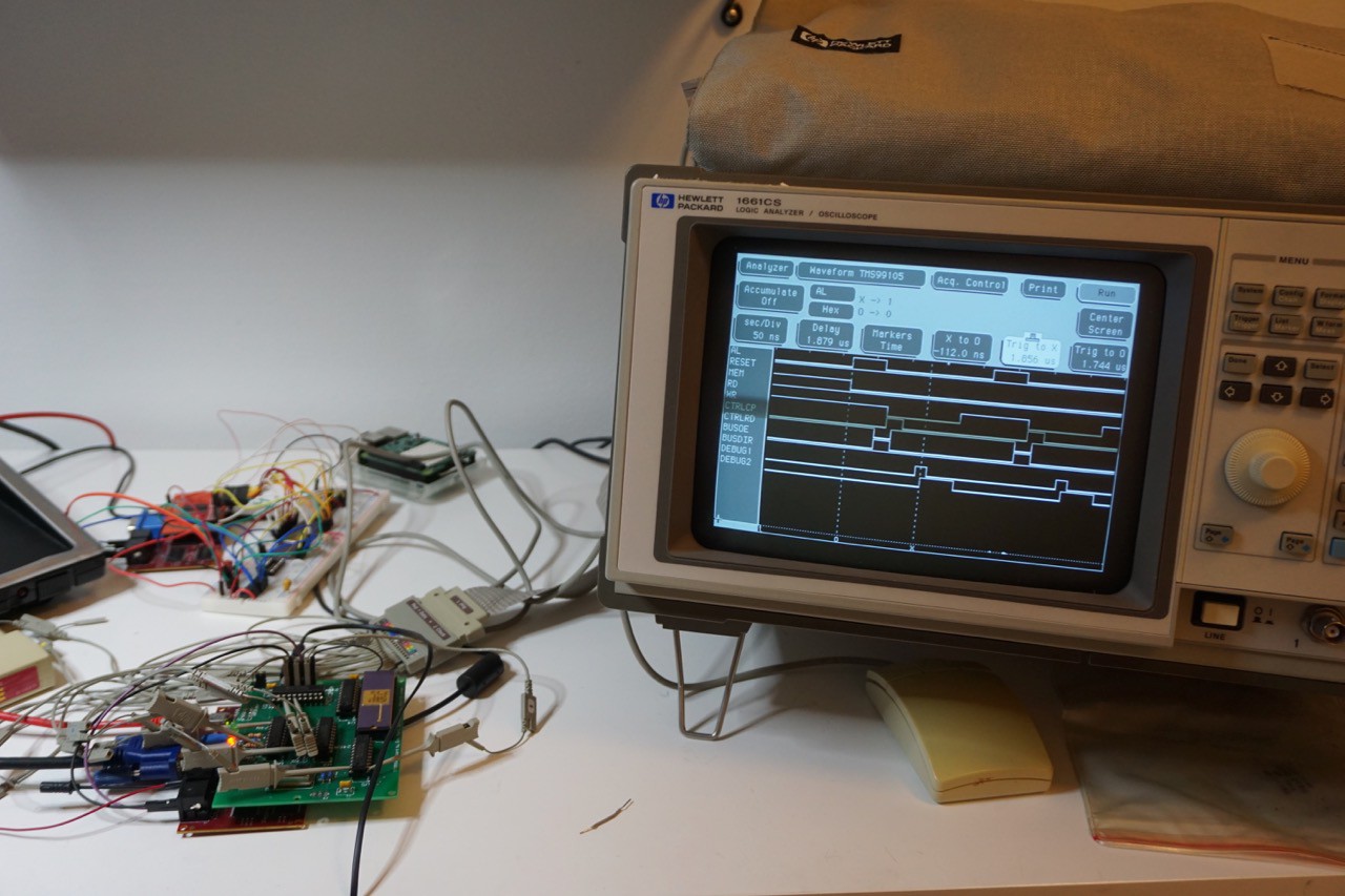
It's been a while since my last update. During the time I haven't had that much time to put into the project. However, there is some nice progress:

I have fully assembled two boards and they work. As can be seen from the picture above, one extra wire is still needed to carry the CPU's write signal to the FPGA. All the other signals are delivered through the pin headers. The two headers carry a limited number of signals: the larger header has 16 signal pins. These are used in a three way multiplexing scheme, timing is based on the CPUs address latch signal. These are the phases:
- Address transfer from CPU to FPGA (early part of the address latch high). This part takes about 30 nanoseconds.
- Control signal transfer from FPGA to CPU and sampling of some CPU signals from the CPU to the FPGA. This takes the next 30 nanoseconds.
- The 16 data signals are treated as two groups of eight during this part of the cycle
- One group is from FPGA to CPU, in practice the FPGA clocks 8 signals to the 74ACT574 flop flops. These signals include CPU reset, interrupt, non-maskable interrupt, and other control signals, including the input for the green LEDs. One of the LEDs is simply toggled when 2^19 clocks of address latch are received and allows us to see that the CPU is running. The other LED is lit when the disk subsystem is active.
- The other 8 signal group is used to sample the status of some control lines of the CPU by the FPGA. A 74LVC245 buffer is driven active to do this. The signals include BST1, BST2, BST3, #MEM and #WR. The last one of these, #WR, appears so late in the cycle that I added the red wire depicted above to be able to continuously sample it, instead of trying to sample it during this control signal transfer window.
- Data transfer either to the CPU (reads) or from the CPU (writes). Writes are simply sampled a few 100MHz clock samples into the cycle when #WR has gone low. For reads the FPGA needs to present the CPU with the data for as long it samples it. That is the reason why the #RD signal is not among the multiplexed control signals but rather available directly to FPGA via the other header, which carries 6 control signals in total. Only two signals from the CPU are directly available via this header: #RD and ALATCH. The remaining 4 signals are control signals driven by the FPGA to control the various buffers and the aforementioned 74ACT574 latch. This part of the cycle takes the remaining 140 nanoseconds or so (a memory cycle is 200ns at 20MHz).
This timing sequence is somewhat visible in the logic analyser picture below:

In the picture there are a few notable signals:
- AL shows the CPU's address latch signal and is the basis of timing
- CTRLCP is the clock driving the 8-bit 74ACT574 register. The FPGA generates this signal once it has sampled the address over during AL high (the sampling occurs over the 16 signal pins).
- CTRLRD enables a 74LVC245 buffer so that the FPGA can read the bus status lines. Active low.
- BUSOE, when low, allows the FPGA to observe or drive the 16-bit multiplexed address/data bus of the CPU.
As can be seen in picture, BUSOE and CTRLRD are effectively the same signal, the other is just an inverted version as the 16 signal bus can only either be used for control signals or the address/data bus. CTRLRD is active for 30 nanoseconds. The rising edge of CTRLCP appears 20 ns into this cycle, to provide enough time for the buffers to settle.
 Erik Piehl
Discussions
Become a Hackaday.io Member
Create an account to leave a comment. Already have an account? Log In.