 Martin Maly
I write a book about old computers. Oh, sorry: I mean "vintage computers" from 80's. My primary goal is to show how one can build a 8bit computer from scratch. It means: how to set up a CPU, how to connect memories, how to connect peripheral chips, and why to connect...
This computer is a "demo construction": A computer, based on 8085 CPU, with 32 kB of (EEP)ROM and 32 kB of RAM, serial connection and parallel ports. All should be as simple as possible. And here is a result.
Wait a moment - why OMEN?
It is simple. OMEN is an abbreviation (of course) of Czech expression "Osmibitový Mikropočítač pro Elektronické Nadšence", which means "an 8bit Microcomputer for Electro Enthusiasts".
Of course - when I have connected the speaker and played a tune, the first tune I have implemented was... right, "The Omen" by Prodigy!
Monitor
Monitor has four commands:
D is for memory dump
M is for memory change
G is for Go
: is for load a HEX file
EEPROM contains TINY BASIC at address 1000h, so enter G1000 to start BASIC.
Programming
As easy, just write a program in assembly language, compile it to the HEX and copy/paste to serial monitor. Then use G command (as GO) to run.
See this video:
LED display and a hexadecimal keyboard
Here is the classic peripheral device for a single board computer: LED 7segment display and a hexadecimal keyboard.
Of course I can use the classic keyboard matrix and some 7segment displays, a bunch of resistors
and transistors and solder a vintage one. Yes, I can, and it's easy. Instead I have used the cheap LED+key module from China. Its type is QYF-TM1638.
This is it:
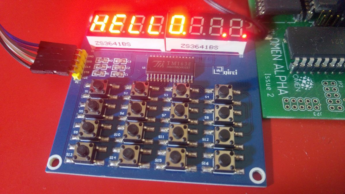
You can buy it on eBay or AliExpress for about 3 USD.
It provides the modern LED display driver and keyboard scanner. It has a serial interface - not an UART, but some kind of SPI with bidirectional data line.
You need three pins to connect this module: strobe pin (output from CPU), clock pin (output from CPU) and data (bidir). So there was a problem: How to achieve a bidir interface in the OMEN Alpha?
I have used the 82C55 parallel interface, port C. Port C can be split into two groups (higher and lower half, PC7-PC4 and PC3-PC0), which can be configured as input or output independently. Ports A and B has the same direction for the whole port.
So I have set the lower half of port C as output for STB and CLK, and the upper one I can switch between input and output. Data pin DIO is connected to port C pin 7.
Here is a source code for the driver. It is not optimized, straightforward and rather ugly, but it works!
OMEN Alpha, issue 2
The second version of PCB has some new features:
- System connector (24 pins) with data bus, A0-A2, /RD and /WR, seven /CS (decoded), system clock and an interrupt
- Selectable IRQ (RST7.5) for external interrupt request
- Switchable /WE for EEPROM to enable in-place programming
PCB - Issue 4
My Tindie shop is out of stock, so I decided to fabricate a new batch of PCBs. I have skipped the Issue 3 (backplane version) and made a new, slightly improved version, Issue 4. The improvements are:
- Signals RESET and READY are added to the application / system bus
- 10k pull-up resistor between READY and Vcc to drive this line with open collector drivers
- Removed the LED and 330R resistor. Three pins are added: SID, SOD and GND to enjoy a serial port.
- One place for 22pF capacitor was removed.
Parts placing on PCB
Here is parts placing image:
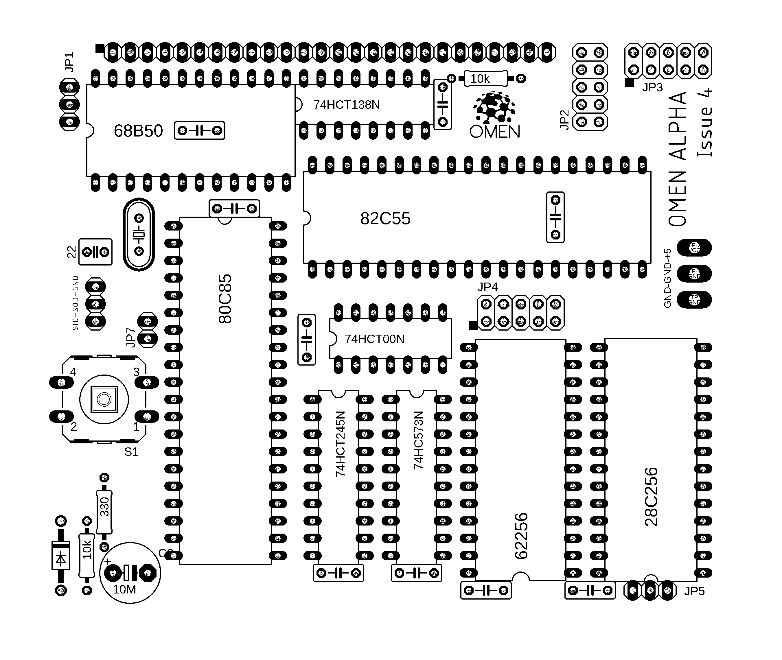
Jumpers etc.
- JP1 is a serial port. Pins are (from bottom to up): GND, TxD, RxD (next to "JP1" label)
- JP2, JP3, JP4: Parallel ports from 8255. A square marks pin 1, see below to schematics. JP2 is port PA, JP3 is for PB, JP4 is for PC
- JP5 is a EEPROM write enable. Connect pins 1-2 to disable writing, connect 2-3 to enable (pin 1 is the leftmost, pin 3 is next to the label "JP5")
- JP7 is RST7.5 enabler. Close to disable interrupt, open to enable.
System connector (at the upper edge, square marks pin 1)
- /WR
- D0
- D1
- D2
- D3
- D4
- D5
- D6
- D7
- A0
- A1
- A2
- /RD
- IO1
- IO2
- IO3
- IO4
- IO5
- IO6
- IO7
- Vcc
- GND
- RST7.5
- CLK
- RESET (output)
- READY (normally 1. Pull down to 0 for processor wait state)
Parallel ports:
Square marks the "Vcc" pin.
JP2:
| GND | PA7 | PA6 | PA5 | PA4 |
| Vcc | PA0 | PA1 | PA2 | PA3 |
JP3:
| GND | PB7 | PB6 | PB5 | PB4 |
| Vcc | PB0 | PB1 | PB2 | PB3 |
JP4:
| GND | PC7 | PC6 | PC5 | PC4 |
| Vcc | PC0 | PC1 | PC2 | PC3 |
Further plans
I plan more OMENs, named Bravo, Charlie, Delta, Echo... Bravo is simillar SBC, but with 65C02 CPU. And other ones? Stay tuned!